Switching characteristics - cs5511/13 – Cirrus Logic CS5513 User Manual
Page 8
CS5510/11/12/13
8
DS337F4
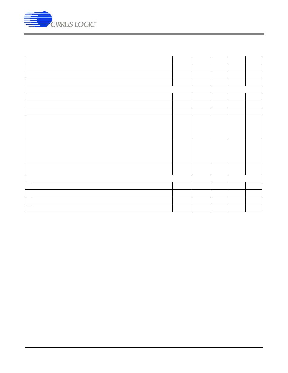
SWITCHING CHARACTERISTICS - CS5511/13
(T
A
= 25° C; V+ = 5 V ±5%; V- = 0 V; Input Levels: Logic 0 = 0 V, Logic 1 = V+; C
L
= 50 pF)
Notes: 23. The internal oscillator in the CS5511/13 provides the master clock for performing conversions. Data is
retrieved from the serial port using the SCLK input pin.
24. The minimum SCLK rate for the CS5511/13 assumes that SCLK is logic 0 when idle. When data is being
read from the ADC, SCLK must be burst at a minimum rate of 10 kHz and with a minimum of a 10
percent duty cycle. Rates slower than this can potentially put the ADC into sleep as the sleep mode is
entered after SCLK is logic 1 for t
SLP
time.
25. On the CS5511/13, the serial clock (SCLK) is used to transfer data from the CS5511/13. If SCLK is held
high (logic 1) for t
SLP
or longer, the CS5511/13 enters sleep mode. To exit from sleep mode, SCLK must
be held low (logic 0) for t
WAKE
or longer.
26. Specified using 10% and 90% points on waveform of interest. Output loaded with 50 pF.
Parameter
Symbol
Min
Typ
Max
Unit
Internal Oscillator Timing
Internal Oscillator Frequency
f
osc
32
64
100
kHz
Internal Oscillator Drift Over Temperature
-
-
-0.02
-
%/°C
Serial Port Timing
Serial Clock Frequency
SCLK
-
-
2
MHz
SCLK High to Enter Sleep
t
SLP
200
-
2000
µs
SCLK Low to Exit Sleep
t
WAKE
10
-
-
µs
Rise Times
CSB
SCLK
SDO
t
rise
-
-
-
-
-
50
1.0
10
-
µs
µs
ns
Fall Times
CSB
SCLK
SDO
t
fall
-
-
-
-
-
50
1.0
10
-
µs
µs
ns
Serial Clock
Pulse Width High
Pulse Width Low
t
6
t
7
200
200
-
-
-
-
ns
ns
SDO Read Timing
CS
to Data Valid
t
8
-
-
150
ns
SCLK Falling to New Data Bit
t
9
-
-
150
ns
CS
Rising to SDO Hi-Z
t
10
-
-
150
ns
CS
Falling to SCLK Rising
t
11
200
-
-
ns