4 digital filter – Cirrus Logic CS5513 User Manual
Page 18
CS5510/11/12/13
18
DS337F4
cessively overranged. If the OD bit is set, the con-
version data bits can be completely erroneous. The
OD flag bit will be cleared to logic 0 four output
words after the modulator becomes stable again.
The OD flag can occur independent of OF with a
spike on the input. Both flag bits should be tested
if any overrange condition occurs.
Table 3 illustrates the output coding for the
CS5510/11/12/13. Conversions are output as
two's complement values representing bipolar in-
put signals.
2.5.4
Digital Filter
The CS5510/11/12/13 have a modified Sinc
4
digi-
tal filter that provides CLK/612 Hz conversion rates
(CLK represents SCLK for the CS5510/12 and the
internal oscillator for the CS5511/13). The filters
are optimized to yield better than 80 dB rejection
between 47 Hz to 63 Hz (i.e. 80 dB minimum rejec-
tion for both 50 Hz and 60 Hz) when the master
clock is 32.768 kHz. The filter has a response as
shown in Figure 20. Table 4 shows the filter re-
sponse for frequencies from 38 Hz to 71 Hz. Note
that the response of the CS5511/13 will be similar,
but the frequencies scale with the on-chip oscilla-
tor’s frequency, which can be from 32 kHz to
96 kHz (i.e. conversion rates can vary between
53 Sps to 159 Sps). Further note that after initial
power up, or after returning from sleep mode, the
filter requires four conversion cycles to produce a
D23
D22
D21
D20
D19
D18
D17
D16
D15
D14
D13
D12
0
OF
OD
0
MSB
18
17
16
15
14
13
12
D11
D10
D9
D8
D7
D6
D5
D4
D3
D2
D1
D0
11
10
9
8
7
6
5
4
3
2
1
LSB
Table 1. CS5512/13 Output Conversion Data Register Description (Flags + 20 bits).
D23
D22
D21
D20
D19
D18
D17
D16
D15
D14
D13
D12
0
OF
OD
0
0
0
0
0
MSB
14
13
12
D11
D10
D9
D8
D7
D6
D5
D4
D3
D2
D1
D0
11
10
9
8
7
6
5
4
3
2
1
LSB
Table 2. CS5510/11 Output Conversion Data Register Description (Flags + 16 bits).
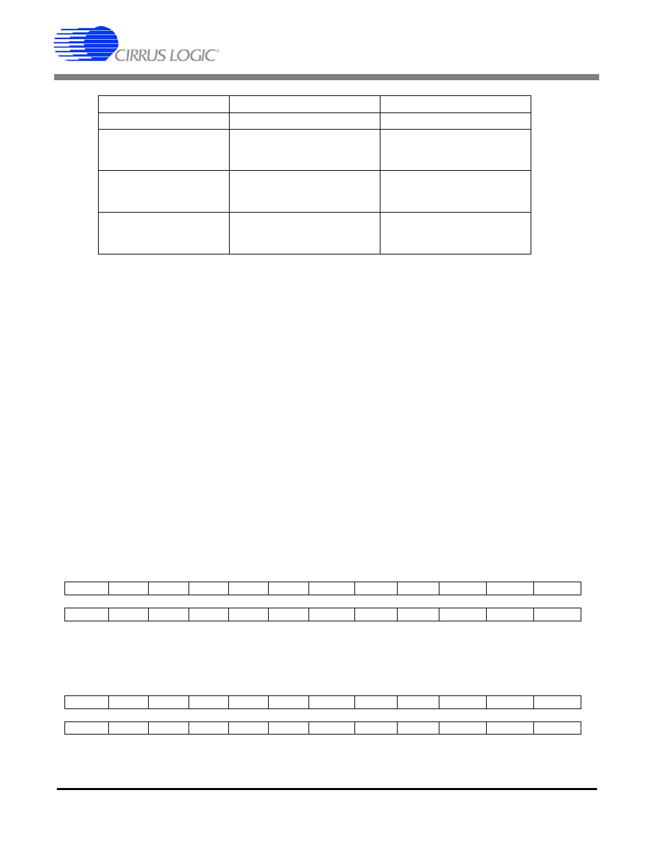
Note: VFS in the table equals the voltage between AIN+ and AIN-. See text about error flags
under overrange conditions.
Table 3. CS5510/11/12/13 Output Coding.
Bipolar Input Voltage
Two's Complement (20-Bit)
Two's Complement (16-Bit)
>(VFS-1.5 LSB)
7FFFF
7FFF
VFS-1.5 LSB
7FFFF
-----
7FFFE
7FFF
-----
7FFE
-0.5 LSB
00000
-----
FFFFF
0000
-----
FFFF
-VFS+0.5 LSB
80001
-----
80000
8001
-----
8000