Digital characteristics, Analog characteristics – Cirrus Logic CS5513 User Manual
Page 5
CS5510/11/12/13
DS337F4
5
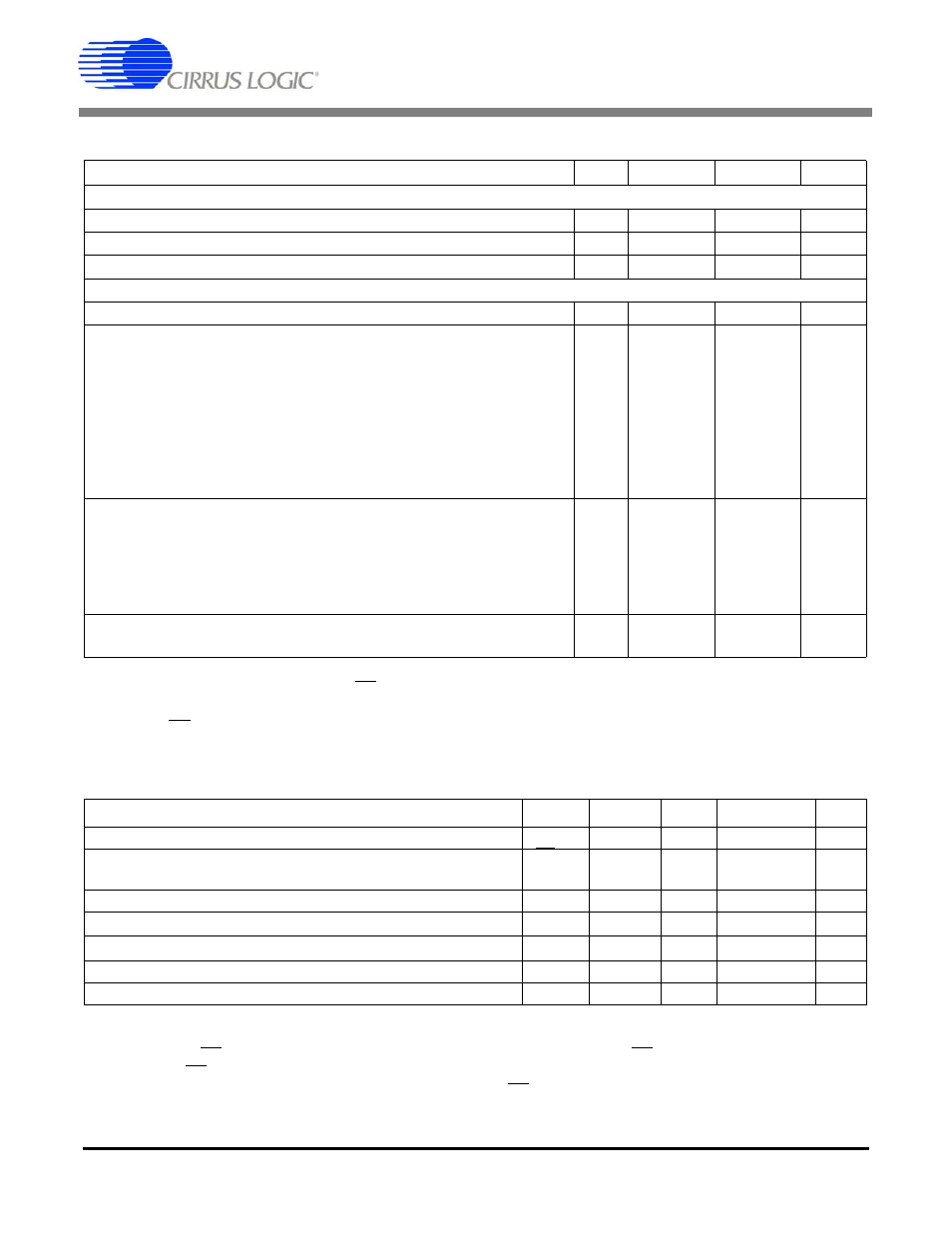
ANALOG CHARACTERISTICS
(Continued)
Notes: 8. VREF is referenced to V- and must be less than or equal to V+.
9. Due to current through the CS pin, I
V+
and I
V-
may not always be the same value.
10. All outputs unloaded. All inputs CMOS levels (> (V+ - 0.6 V) or < (V- + 0.6 V)).
11. CS must be inactive (logic high) during sleep to meet this power specification.
DIGITAL CHARACTERISTICS
(T
A
= 25° C; V
+ = 5 V ±5%; V- = 0 V) (See Notes 1 and 12.)
Notes: 12. All measurements performed under static conditions.
13. V
L1
is 0.5 (V+ - V-) + 0.6 V + V-.
14. The CS signal provides the sink current path for the SDO pin when CS is low. The external drive logic
to CS, therefore, must be able to handle the logic-low current drive levels for all devices attached to
SDO. The voltage specified for SDO is relative to CS
Low
. See Section 2.3.1, “Digital Logic Levels” and
Figure 11 for more details.
Parameter
Min
Typ
Max
Unit
Voltage Reference Input
Range
{(VREF) - (V-)}
(Note 8) 0.250
2.5
(V+) - (V-)
V
Input Capacitance
-
7
-
pF
CVF current
-
6
-
nA
Power Supplies
Supply Voltages
{(V+) - (V-)}
4.75
5
5.25
V
DC Power Supply Currents
(Note 9)
I
V+
CS5510
CS5511
CS5512
CS5513
I
V-
CS5510
CS5511
CS5512
CS5513
-
-
-
-
-
-
-
-
275
290
360
385
275
290
360
385
360
380
470
500
360
380
470
500
µA
µA
µA
µA
µA
µA
µA
µA
Power Consumption
(Note 10)
CS5510
CS5511
CS5512
CS5513
Sleep
-
-
-
-
-
1.4
1.5
1.8
1.9
10
1.9
2.0
2.5
2.7
-
mW
mW
mW
mW
µW
Power Supply Rejection
dc Positive Supply
dc Negative Supply
-
-
85
85
-
-
dB
dB
Parameter
Symbol
Min
Typ
Max
Unit
High-Level Input Voltage:
CS and SCLK
V
IH
V+ - 0.45
-
-
V
Low-Level Input Voltage:
(Note 13)
CS
SCLK
CS
Low
V
IL
-
-
-
-
V
L1
V
L1
V
V
Input Current:
(Note 14)
CS
I
CS
-
-
1.0
mA
High-Level Output Voltage:
SDO, I
source
= 5.0mA
V
OH
(V+) - 0.6
-
-
V
Low-Level Output Voltage:
(Note 14) SDO, I
sink
= 1.0mA
V
OL
-
-
(
CS
Low
) + 0.6
V
Input Leakage Current
SCLK
I
in
-
±0.015
±10
µA
3-State Leakage Current
SCLK
I
OZ
-
-
±10
µA