1 voltage reference input model, 3 power supply arrangements, 1 digital logic levels – Cirrus Logic CS5513 User Manual
Page 11: E section 2.3.1, “digital logic levels” an
CS5510/11/12/13
DS337F4
11
CS5512/13. The CS5510/11 follow the same
curve, but are limited to 16 bits of resolution. Note
that the reference voltage should not be estab-
lished prior to having the supply voltages on the V+
and V- pins.
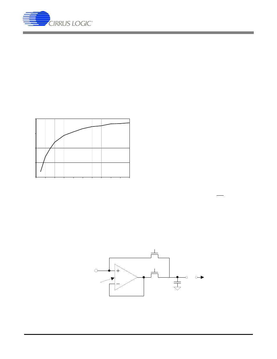
2.2.1
Voltage Reference Input Model
Figure 5 illustrates the input model for the VREF
pin. It includes a coarse/fine charge buffer which
reduces the dynamic current demand of the exter-
nal reference. Typical CVF (sampling) current is
about 6 nA (See Figure 5).
The nominal input span of the converter is defined
to be a bipolar span equal to ±(VREF - V-)*(0.80
±0.08).
2.3
Power Supply Arrangements
The CS5510/11/12/13 are designed to operate
from single or dual supplies. Figure 6 illustrates the
CS5510/11/12/13 connected with a single +5 V
supply to measure differential inputs relative to a
common mode of 2.5 V. Figure 7 illustrates the
CS5510/11/12/13 connected with ±2.5 V analog
supplies to measure ground-referenced, bipolar
signals. It is not necessary that the dual supples on
the ADCs be balanced, however, they must sum to
five volts. Figure 8 illustrates the ADCs configured
with V+ = +3.3 V and V- = -1.7 V, accommodating
a +3.3 V digital supply.
2.3.1
Digital Logic Levels
The many power supply configurations available in
the CS5510/11/12/13 allow for a wide range of dig-
ital logic levels. The logic-high input and output lev-
els are determined by the V+ pin. The logic-low
output on SDO is referenced to and driven by the
current logic-low voltage on CS. Since the
CS5510/11/12/13 do not include a dedicated
13
14
15
16
17
0
0.5
1
1.5
2
2.5
3
3.5
4
4.5
5
VREF (V)
Effective Bits
Figure 4. CS5512/13 Measured Noise-Free Bits vs.
VREF.
VREF
C = 7 p F
2
φ
1
φ
V
≤ 2 5 mV
o s
i
= f V
C
o s
n
f = 32.768 kHz
Coarse
Fine
Figure 5. Input model for VREF pin.