Switching characteristics, Cs5466 – Cirrus Logic CS5466 User Manual
Page 8
CS5466
8
DS659F2
SWITCHING CHARACTERISTICS
•
Min / Max characteristics and specifications are guaranteed over all operating conditions.
•
Typical characteristics and specifications are measured at nominal supply voltages and TA = 25 °C.
•
VA+ = 5 V ±5% VD+ = 3.3 V ±5% or 5 V ±5%; AGND = DGND = 0 V. All voltages with respect to 0 V.
•
Logic Levels: Logic 0 = 0 V, Logic 1 = VD+.
Notes:
11.
Specified using 10% and 90% points on wave-form of interest. Output loaded with 50 pF.
12.
Oscillator start-up time varies with crystal parameters. This specification does not apply when using an external
clock source.
13.
Pulse output timing is specified at MCLK = 4.096 MHz. Current and voltage signals are at unity power factor. See
on page 11. for more information on pulse output pins.
14.
Timing is proportional to the frequency of MCLK.
15.
When FREQ2 = 0, FREQ1=1 and FREQ0=1, FOUT will have a typical pulse width of 20
s at MCLK = 4.096 MHz.
Parameter
Symbol Min Typ
Max
Unit
Rise Times
Digital Output (Note 11)
t
rise
-
50
-
ns
Fall Times
Digital Output (Note 11)
t
fall
-
50
-
ns
Start-up
Oscillator Start-up Time
XTAL = 4.096 MHz (Note 12)
t
ost
-
60
-
ms
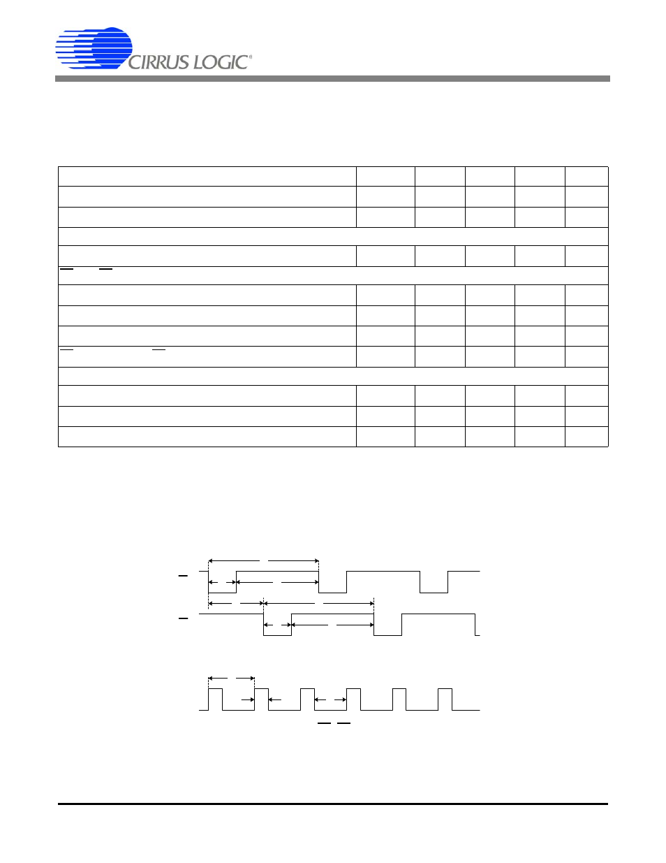
E1 and E2 Timing (Note 13 and 14)
Period
t
1
500
-
-
ms
Pulse Width
t
2
250
-
-
ms
Rising Edge to Falling Edge
t
3
250
-
-
ms
E1 Falling Edge to E2 Falling Edge
t
4
250
-
-
ms
FOUT Timing (Note 13 and 14)
Period
t
5
0.10
1 / f
FOUT
ms
Pulse Width
t
6
-
0.5*t
5
90
ms
FOUT Low
t
7
-
0.5*t
5
-
ms
E1
E2
FOUT
t
1
t
2
t
3
t
5
t
6
t
4
t
7
t
3
t
1
t
2
Figure 1. Timing Diagram for E1, E2 and FOUT (Not to Scale)