5 e1 and e2 frequency calculation, 4 energy direction indicator, 5 power-on reset – Cirrus Logic CS5466 User Manual
Page 13: 6 oscillator characteristics, Figure 3. oscillator connection, Cs5466
CS5466
DS659F2
13
5.3.5
E1 and E2 Frequency Calculation
The pulse output frequency of E1 and E2 is directly pro-
portional to the active power calculated from the input
signals. To calculate the output frequency on E1 and
E2, use the following transfer function:
Example:
For a given application, assume a 50 Hz line frequency
and a purely resistive load (unity power factor), the fol-
lowing configuration is used:
– FREQ[2:0] = 3
FREQ
max
= 2 Hz
– IGAIN[1:0] = 2
IGAIN = 100
– VREFIN = VREFOUT = 2.5 V
In this configuration, the maximum sine wave that can
be applied is 250 mVp on the voltage channel and
25 mVp on the current channel. Using the above equa-
tion, the output frequency of energy pulse E1 or E2 is
calculated:
With maximum pure sinusoidal input signals, the fre-
quency of E1 or E2 is half the absolute maximum fre-
quency set with FREQ[2:0].
To calculate the frequency of FOUT for the example
above, assume FREQ2 = 0.
5.4
Energy Direction Indicator
The NEG pin indicates the sign of the calculated active
power. If negative active power is detected, the NEG
output pin will become active-high and will remain ac-
tive-high until positive active power is detected. The
NEG pin is valid at least 250ns prior to any assertion of
E1 or E2, and FOUT, to indicate the sign of a given en-
ergy output. The NEG pin is updated at a rate of 10 Hz
at MCLK = 4.096 MHz.
5.5
Power-on Reset
Upon powering up, the digital circuitry is held in reset
until the analog voltage reaches 4.0 V. At that time, an
eight-XIN-clock-period delay is enabled to allow the os-
cillator to stabilize. The CS5466 will then initialize. The
device reads the control pins IGAIN[1:0], FREQ[2:0]
and HPF, and begins performing energy measure-
ments.
5.6
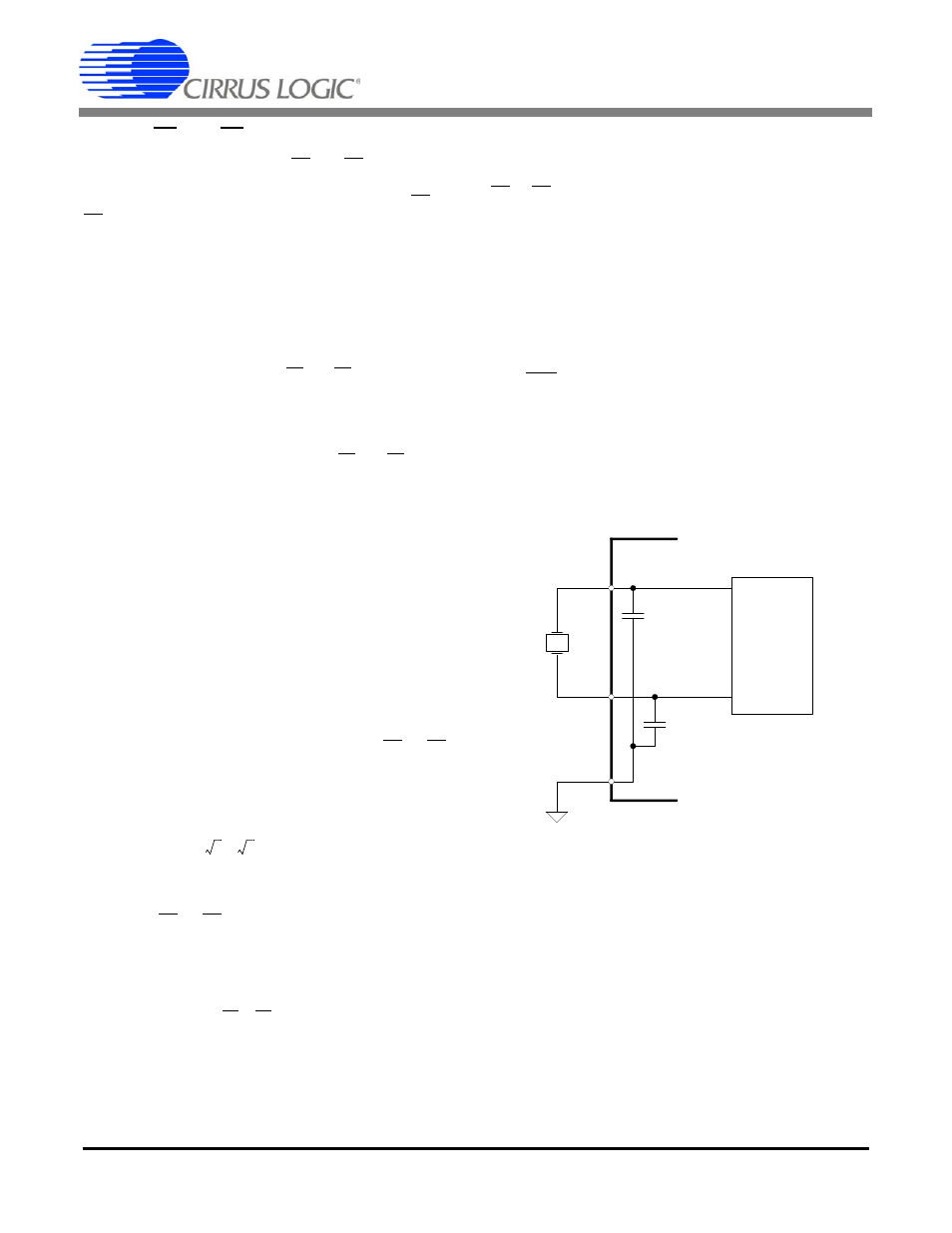
Oscillator Characteristics
XIN and XOUT are the input and output of an inverting
amplifier which can be configured as an on-chip oscilla-
tor, as shown in
. The oscillator circuit is de-
signed to work with a quartz crystal. To reduce circuit
cost, two load capacitors C1 and C2 are integrated in
the device, one between XIN and DGND and the other
between XOUT and DGND. Lead lengths to/from the
crystal should be minimized to reduce stray capaci-
tance. To drive the device from an external clock
source, XOUT should be left unconnected while XIN is
driven by the external circuitry. There is an amplifier be-
tween XIN and the digital section which provides
CMOS-level signals. This amplifier works with sinusoi-
dal inputs so there are no problems with slow edge
times.
FREQ
E1,E2
= Actual frequency of E1 and E2 pulses [Hz]
VIN = rms voltage across VIN+ and VIN- [V]
IIN = rms voltage across IIN+ and IIN- [V]
IGAIN = Current channel gain selection (10, 50, 100, 150)
PF = Power Factor
FREQ
max
= Absolute Max Frequency for E1 and E2 [Hz]
VREFIN = Voltage at VREFIN pin [V]
FREQ
E1,E2
VIN
10
IIN
IGAIN
PF
FREQ
max
VREFIN
2
------------------------------------------------------------------------------------------------------------------
=
0.25V
p
10
0.025V
p
100
1
2Hz
2
2
2.5V
2
---------------------------------------------------------------------------------------------------------
1Hz
=
FOUT
2048
E1
E2
+
2048
2Hz
4096Hz
=
=
=
Oscillator
Circuit
DGND
XIN
XOUT
C1
C1 =
22 pF
C2
C2 =
Figure 3. Oscillator Connection