Voltage reference, Digital characteristics, Cs5463 – Cirrus Logic CS5463 User Manual
Page 9
CS5463
DS678F3
9
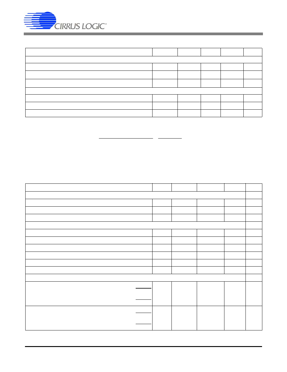
VOLTAGE REFERENCE
Notes: 8. The voltage at VREFOUT is measured across the temperature range. From these measurements the
following formula is used to calculate the VREFOUT Temperature Coefficient:.
9. Specified at maximum recommended output of 1 µA, source or sink.
DIGITAL CHARACTERISTICS
•
Min / Max characteristics and specifications are guaranteed over all
Recommended Operating Conditions
•
Typical characteristics and specifications are measured at nominal supply voltages and TA = 25 °C.
•
VA+ = VD+ = 5V ±5%; AGND = DGND = 0 V. All voltages with respect to 0 V.
•
MCLK = 4.096 MHz.
Parameter
Symbol Min Typ
Max
Unit
Reference Output
Output Voltage
VREFOUT
+2.4
+2.5
+2.6
V
Temperature Coefficient
TC
VREF
-
25
60
ppm/°C
Load Regulation
V
R
-
6
10
mV
Reference Input
Input Voltage Range
VREFIN
+2.4
+2.5
+2.6
V
Input Capacitance
-
4
-
pF
Input CVF Current
-
25
-
nA
Parameter
Symbol Min
Typ
Max
Unit
Master Clock Characteristics
Master Clock Frequency
Internal Gate Oscillator (Note 11) MCLK
2.5
4.096
20
MHz
Master Clock Duty Cycle
40
-
60
%
CPUCLK Duty Cycle
40
-
60
%
Filter Characteristics
Phase Compensation Range
(Voltage Channel, 60 Hz)
-2.8
-
+2.8
°
Input Sampling Rate
DCLK = MCLK/K
-
DCLK/8
-
Hz
Digital Filter Output Word Rate
(Both Channels)
OWR
-
DCLK/1024
-
Hz
High-pass Filter Corner Frequency
-3 dB
-
0.5
-
Hz
Full-scale DC Calibration Range (
Referred to Input
) (Note 14) FSCR
25
-
100
%F.S.
Channel-to-channel Time-shift Error
1.0
µs
Input/Output Characteristics
High-level Input Voltage
All Pins Except XIN and SCLK and RESET
XIN
SCLK and RESET
V
IH
0.6 VD+
(VD+) - 0.5
0.8
VD+
-
-
-
-
-
-
V
V
V
Low-level Input Voltage (VD = 5 V)
All Pins Except XIN and SCLK and RESET
XIN
SCLK and RESET
V
IL
-
-
-
-
-
-
0.8
1.5
0.2
VD+
V
V
V
(VREFOUT
MAX
- VREFOUT
MIN
)
VREFO UT
AVG
(
(
1
T
A
MAX
- T
A
M IN
(
(
1.0 x 10
(
(
6
TC
VREF
=