Pin description, Cs5463 – Cirrus Logic CS5463 User Manual
Page 6
CS5463
6
DS678F3
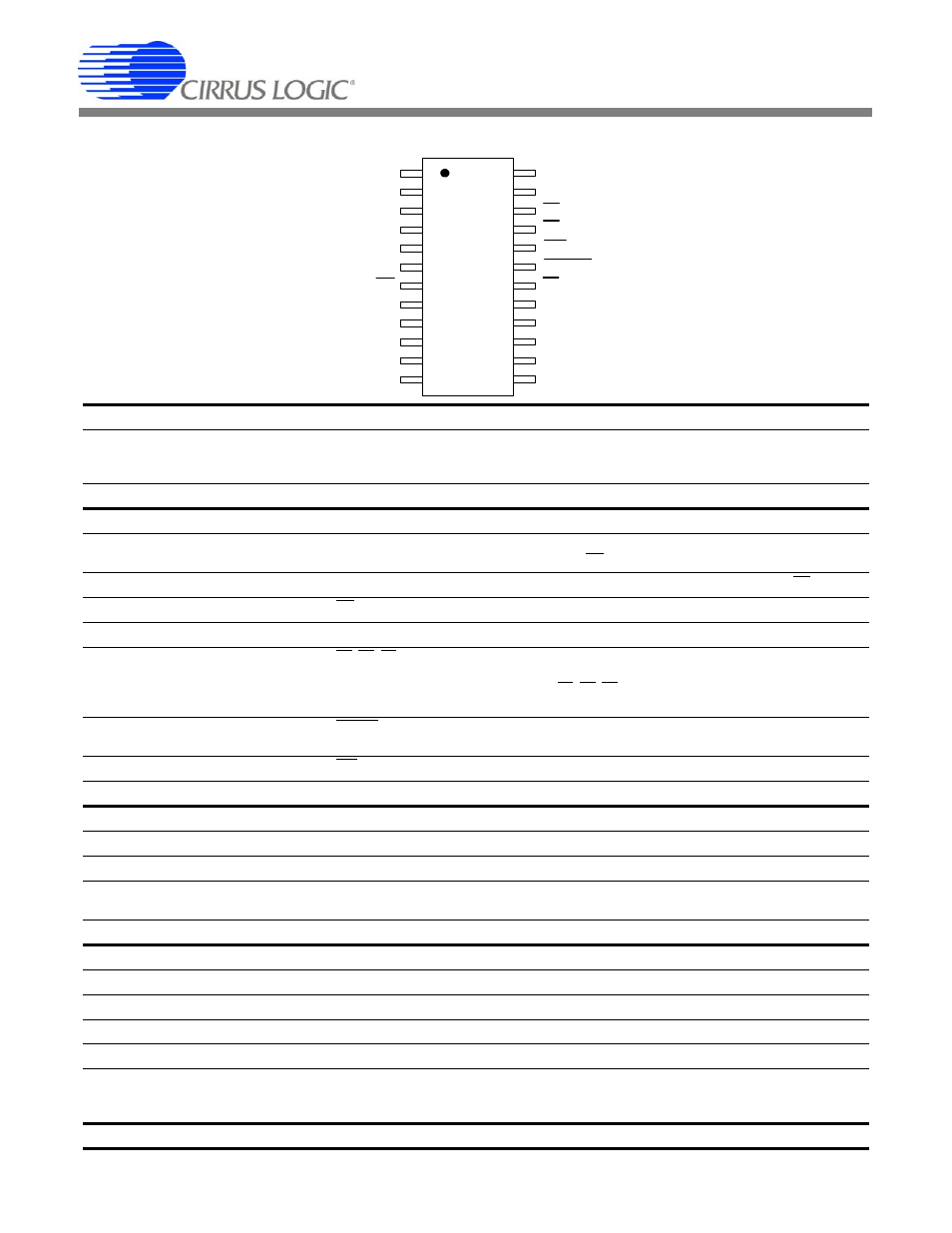
2. PIN DESCRIPTION
Clock Generator
Crystal Out
Crystal In
1,24
XOUT, XIN – The output and input of an inverting amplifier. Oscillation occurs when connected to
a crystal, providing an on-chip system clock. Alternatively, an external clock can be supplied to
the XIN pin to provide the system clock for the device.
CPU Clock Output
2
CPUCLK – Output of on-chip oscillator which can drive one standard CMOS load.
Control Pins and Serial Data I/O
Serial Clock Input
5
SCLK – A Schmitt-trigger input pin. Clocks data from the SDI pin into the receive buffer and out
of the transmit buffer onto the SDO pin when CS is low.
Serial Data Output
6
SDO – Serial port data output pin.SDO is forced into a high-impedance state when CS is high.
Chip Select
7
CS – Low, activates the serial port interface.
Mode Select
8
MODE - High, enables the “auto-boot” mode. The mode pin has an internal pull-down resistor.
Energy Output
18,21,22
E3, E1, E2 – Active-low pulses with an output frequency proportional to the selected power. Con-
figurable outputs for active, apparent, and reactive power, negative energy indication, zero cross
detection, and power failure monitoring. E1, E2, E3 outputs are configured in the Operational
Modes Register.
Reset
19
RESET – A Schmitt-trigger input pin. Low activates Reset, all internal registers (some of which
drive output pins) are set to their default states.
Interrupt
20
INT - Low, indicates that an enabled event has occurred.
Serial Data Input
23
SDI - Serial port data input pin. Data will be input at a rate determined by SCLK.
Analog Inputs/Outputs
Differential Voltage Inputs
9,10
VIN+, VIN- – Differential analog input pins for the voltage channel.
Differential Current Inputs
15,16
IIN+, IIN- – Differential analog input pins for the current channel.
Voltage Reference Output
11
VREFOUT – The on-chip voltage reference output. The voltage reference has a nominal magni-
tude of 2.5 V and is referenced to the AGND pin on the converter.
Voltage Reference Input
12
VREFIN – The input to this pin establishes the voltage reference for the on-chip modulator.
Power Supply Connections
Positive Digital Supply
3
VD+ – The positive digital supply.
Digital Ground
4
DGND – Digital Ground.
Positive Analog Supply
14
VA+ – The positive analog supply.
Analog Ground
13
AGND – Analog ground.
Power Fail Monitor
1
7
PFMON – The power fail monitor pin monitors the analog supply. If the analog supply does not
meet or falls below PFMON’s voltage threshold, a Low-supply Detect (LSD) event is set in the
status register.
12
11
10
9
8
7
6
5
4
3
2
1
13
14
15
16
17
18
19
20
21
22
23
24
AGND
Analog Ground
VA+
Positive Analog Supply
IIN-
Differential Current Input
IIN+
Differential Current Input
PFMON Power Fail Monitor
E3
High Frequency Energy Output
RESET
Reset
INT
Interrupt
E1
Energy Output 1
SDI
Serial Data Input
XIN
Crystal In
E2
Energy Output 2
VREFIN
Voltage Reference Input
VREFOUT
Voltage Reference Output
VIN-
Differential Voltage Input
VIN+
Differential Voltage Input
MODE
Mode Select
CS
Chip Select
SDO
Serial Data Ouput
SCLK
Serial Clock
DGND
Digital Ground
VD+
Positive Digital Supply
CPUCLK
CPU Clock Output
XOUT
Crystal Out