Theory of operation, 1 digital filters, 2 voltage and current measurements – Cirrus Logic CS5463 User Manual
Page 14: 3 power measurements, Figure 3. data measurement flow diagram, Cs5463, And i, Using v, And v
CS5463
14
DS678F3
4. THEORY OF OPERATION
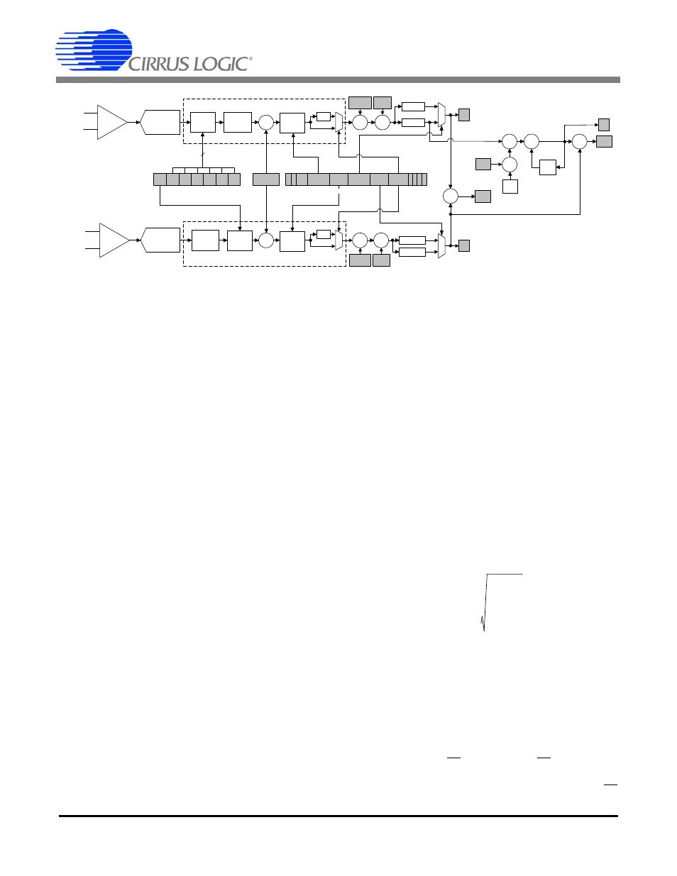
The CS5463 is a dual-channel analog-to-digital convert-
er (ADC) followed by a computation engine that per-
forms power calculations and energy-to-pulse
conversion. The data flow for the voltage and current
channel measurement and the power calculation algo-
rithms are depicted in Figure 3 and 4, respectively.
The analog inputs are structured with two dedicated
channels, Voltage and Current, then optimized to simpli-
fy interfacing to various sensing elements.
The voltage-sensing element introduces a voltage
waveform on the voltage channel input VIN± and is sub-
ject to a gain of 10x. A second-order delta-sigma modu-
lator samples the amplified signal for digitization.
Simultaneously, the current-sensing element introduces
a voltage waveform on the current channel input IIN±
and is subject to two selectable gains of the program-
mable gain amplifier (PGA). The amplified signal is
sampled by a fourth-order delta-sigma modulator for
digitization. Both converters sample at a rate of
MCLK/8, the over-sampling provides a wide dynamic
range and simplified anti-alias filter design.
4.1 Digital Filters
The decimating digital filters on both channels are Sinc
3
filters followed by 4th-order IIR filters. The single-bit
data is passed to the low-pass decimation filter and out-
put at a fixed word rate. The output word is passed to an
optional IIR filter to compensate for the magnitude roll
off of the low-pass filtering operation.
An optional digital high-pass filter (HPF in Figure 3) re-
moves any DC component from the selected signal
path. By removing the DC component from the voltage
and/or the current channel, any DC content will also be
removed from the calculated active power as well. With
both HPFs enabled the DC component will be removed
from the calculated V
RMS
and I
RMS
as well as the appar-
ent power.
When the optional HPF in either channel is disabled, an
all-pass filter (APF) is implemented. The APF has an
amplitude response that is flat within the channel band-
width and is used for matching phase in systems where
only one HPF is engaged.
4.2 Voltage and Current Measurements
The digital filter output word is then subject to a DC off-
set adjustment and a gain calibration (See Section 7.
on page 37). The calibrated mea-
surement is available by reading the instantaneous volt-
age and current registers.
The Root Mean Square (RMS in Figure 4) calculations
are performed on N instantaneous voltage and current
samples, V
n
and I
n
, respectively (where N is the cycle
count), using the formula:
and likewise for V
RMS
, using V
n
. I
RMS
and V
RMS
are ac-
cessible by register reads, which are updated once ev-
ery cycle count (referred to as a computational cycle).
4.3 Power Measurements
The instantaneous voltage and current samples are
multiplied to obtain the instantaneous power (see Fig-
ure 3). The product is then averaged over N conver-
sions to compute active power and is used to drive
energy pulse output E1. Energy output E2 is selectable,
providing an energy sign or a pulse output that is pro-
portional to the apparent power. Energy output E3
VOLTAGE
SINC3
+
X
V
*
gn
CURRENT
SINC3
+
X
I
*
gn
DELAY
REG
DELAY
REG
I
DCoff
*
V
DCoff
*
PGA
+
+
Configuration Register *
Digital Filter
Digital Filter
HPF
2nd Order
Modulator
4th Order
Modulator
x10
X
X
SYS
Gain
*
PC6 PC5 PC4 PC3 PC2 PC1 PC0
6
*DENOTES REGISTER NAME.
DELAY
REG
DELAY
REG
HPF
V
Q
*
XVDEL XIDEL
0
1
2
2322
8
7
...
Operational Modes Register *
+
X
+
X
X
Q*
2
MU
X
X
V *
P*
I *
MU
X
VHPF
IHPF
6
5
*
APF
HPF
APF
MU
X
IIR
MUX
IIR
3
IIR
4
Figure 3. Data Measurement Flow Diagram.
I
RMS
I
n
n
0
=
N
1
–
N
---------------------
=