Register description, 1 configuration register ( config ), Cs5463 – Cirrus Logic CS5463 User Manual
Page 26
CS5463
26
DS678F3
6. REGISTER DESCRIPTION
1. “Default” = bit status after power-on or reset
2. Any bit not labeled is Reserved. A zero should always be used when writing to one of these bits.
6.1 Page 0 Registers
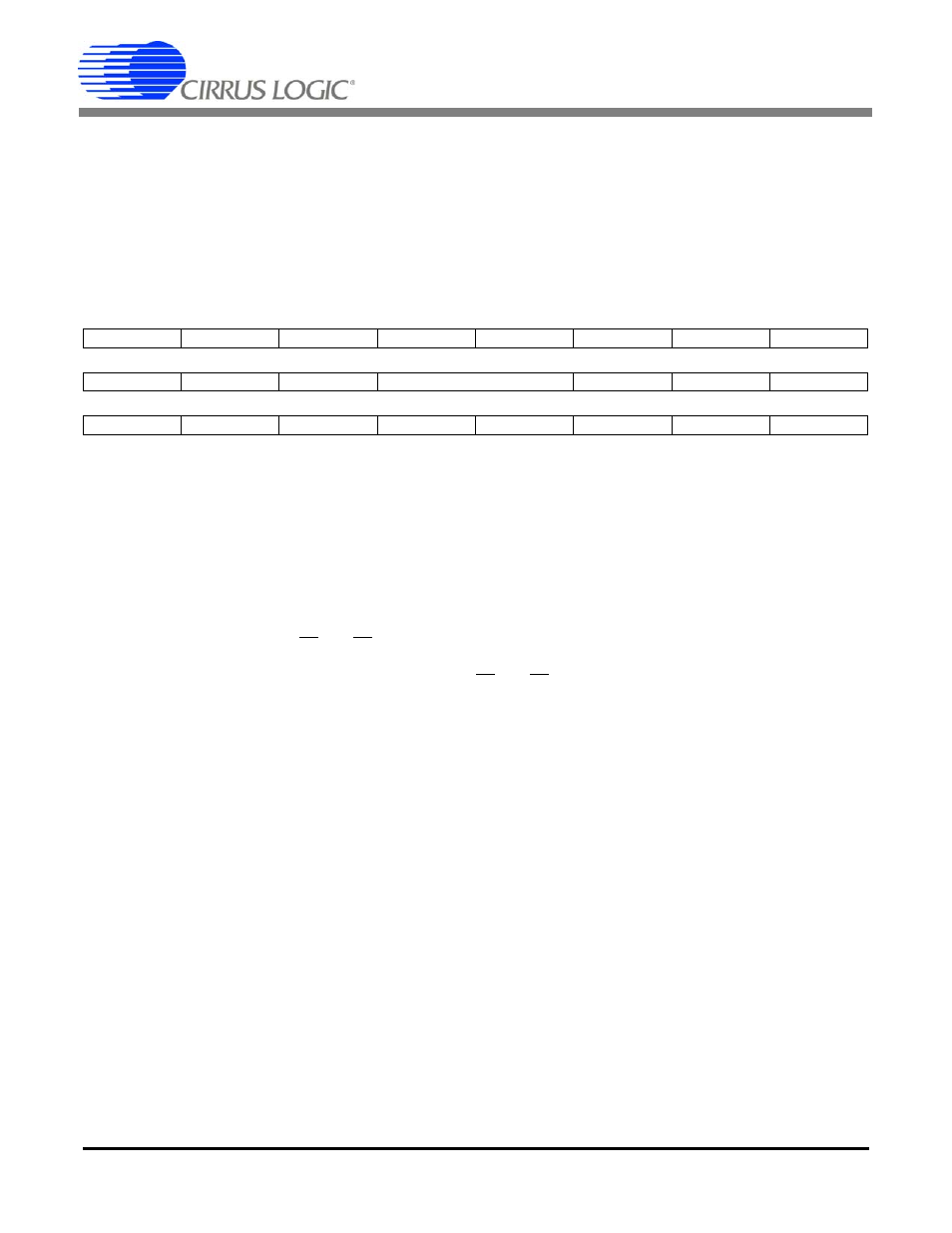
6.1.1 Configuration Register ( Config )
Address: 0
Default = 0x000001
PC[6:0]
Phase compensation. A 2’s complement number which sets a delay in the voltage channel rel-
ative to the current channel. Default setting is 0000000 = 0.0215 degree phase delay at 60 Hz
(when MCLK = 4.096 MHz). See Section 7.2
on page 39 for more infor-
mation.
I
gain
Sets the gain of the current PGA.
0 = Gain is 10 (default)
1 = Gain is 50
EWA
Allows the E1 and E2 pins to be configured as open-collector output pins.
0 = Normal outputs (default)
1 = Only the pull-down device of the E1 and E2 pins are active
IMODE, IINV
Interrupt configuration bits. Select the desired pin behavior for indication of an interrupt.
00 = Active-low level (default)
01 = Active-high level
10 = High-to-low pulse
11 = Low-to-high pulse
iCPU
Inverts the CPUCLK clock. In order to reduce the level of noise present when analog signals
are sampled, the logic driven by CPUCLK should not be active during the sample edge.
0 = Normal operation (default)
1 = Minimize noise when CPUCLK is driving rising edge logic
K[3:0]
Clock divider. A 4-bit binary number used to divide the value of MCLK to generate the internal
clock DCLK. The internal clock frequency is DCLK = MCLK/K. The value of K can range be-
tween 1 and 16. Note that a value of “0000” will set K to 16 (not zero). K = 1 at reset.
23
22
21
20
19
18
17
16
PC6
PC5
PC4
PC3
PC2
PC1
PC0
Igain
15
14
13
12
11
10
9
8
EWA
-
-
IMODE
IINV
-
-
-
7
6
5
4
3
2
1
0
-
-
-
iCPU
K3
K2
K1
K0