Cirrus Logic CS53L21 User Manual
Cs53l21, Low power, stereo analog to digital converter, Features
Copyright
© Cirrus Logic, Inc. 2006
(All Rights Reserved)
Preliminary Product Information
This document contains information for a new product.
Cirrus Logic reserves the right to modify this product without notice.
MAY ‘06
DS700PP1
Low Power, Stereo Analog to Digital Converter
FEATURES
98 dB Dynamic Range (A-wtd)
-88 dB THD+N
Analog Gain Controls
– +32 dB or +16 dB MIC Pre-Amplifiers
– Analog Programmable Gain Amplifier
(PGA)
+20 dB Digital Boost
Programmable Automatic Level Control (ALC)
– Noise Gate for Noise Suppression
– Programmable Threshold and
Attack/Release Rates
Independent Left/Right Channel Control
Digital Volume Control
High-Pass Filter Disable for DC Measurements
Stereo 3:1 Analog Input MUX
Dual MIC Inputs
– Programmable, Low Noise MIC Bias Levels
– Differential MIC Mix for Common Mode
Noise Rejection
Very Low 64 Fs Oversampling Clock Reduces
Power Consumption
SYSTEM FEATURES
24-bit Conversion
4 kHz to 96 kHz Sample Rate
Multi-bit Delta Sigma Architecture
Low Power Operation
– Stereo Record (ADC): 8.72 mW @ 1.8 V
– Stereo Record (MIC to PGA and ADC):
13.73 mW @ 1.8 V
Variable Power Supplies
– 1.8 V to 2.5 V Digital & Analog
– 1.8 V to 3.3 V Interface Logic
Power Down Management
– ADC, MIC Pre-Amplifier, PGA
Software Mode (I²C
®
& SPI
™
Control)
Hardware Mode (Stand-Alone Control)
Flexible Clocking Options
– Master or Slave Operation
Digital Routing Mixes
– Mono Mixes
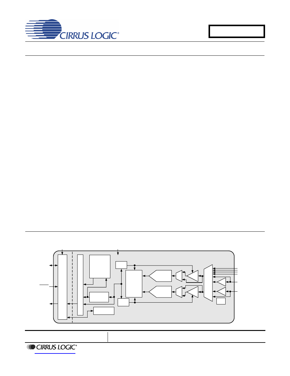
1.8 V to 3.3 V
Multibit
Oversampling
ADC
Multibit
Oversampling
ADC
Serial Audio
Output
1.8 V to 2.5 V
MUX
PGA
PCM
Seri
al
In
te
rf
a
ce
Register
Configuration
Le
ve
l Translato
r
Reset
Software Mode
Stereo Input 1
Stereo Input 2
Stereo Input 3 /
Mic Input 1 & 2
PGA
+32 dB
+32 dB
Volume
Controls
ALC
MIC
Bias
MUX
MUX
High Pass
Filters
ALC
Digital
Signal
Processing
Engine
Hardware Mode
or I
2
C & SPI
Control Data
CS53L21
Document Outline
- 1. Pin Descriptions - Software (Hardware) Mode
- 2. Typical Connection Diagrams
- 3. Characteristic and Specification Tables
- Specified Operating Conditions
- Absolute Maximum Ratings
- Analog Characteristics (Commercial - CNZ)
- Analog Characteristics (Automotive - DNZ)
- ADC Digital Filter Characteristics
- Switching Specifications - Serial Port
- Switching Specifications - I·C Control Port
- Switching Characteristics - SPI Control Port
- DC Electrical Characteristics
- Digital Interface Specifications & Characteristics
- Power Consumption
- 4. Applications
- 4.1 Overview
- 4.2 Hardware Mode
- 4.3 Analog Inputs
- 4.4 Signal Processing Engine
- 4.5 Serial Port Clocking
- 4.6 Digital Interface Formats
- 4.7 Initialization
- 4.8 Recommended Power-Up Sequence
- 4.9 Recommended Power-Down Sequence
- 4.10 Software Mode
- 5. Register Quick Reference
- 6. Register Description
- 6.1 Chip I.D. and Revision Register (Address 01h) (Read Only)
- 6.2 Power Control 1 (Address 02h)
- 6.3 MIC Power Control & Speed Control (Address 03h)
- 6.4 Interface Control (Address 04h)
- 6.5 MIC Control (Address 05h)
- 6.6 ADC Control (Address 06h)
- 6.7 ADCx Input Select, Invert & Mute (Address 07h)
- 6.8 SPE Control (Address 09h)
- 6.9 ALCX & PGAX Control: ALCA, PGAA (Address 0Ah) & ALCB, PGAB (Address 0Bh)
- 6.10 ADCx Attenuator: ADCA (Address 0Ch) & ADCB (Address 0Dh)
- 6.11 ADCx Mixer Volume Control: ADCA (Address 0Eh) & ADCB (Address 0Fh)
- 6.12 Channel Mixer (Address 18h)
- 6.13 ALC Enable & Attack Rate (Address 1Ch)
- 6.14 ALC Release Rate (Address 1Dh)
- 6.15 ALC Threshold (Address 1Eh)
- 6.16 Noise Gate Configuration & Misc. (Address 1Fh)
- 6.17 Status (Address 20h) (Read Only)
- 7. Analog Performance Plots
- 8. Example System Clock Frequencies
- 9. PCB Layout Considerations
- 10. Digital Filters
- 11. Parameter Definitions
- 12. Package Dimensions
- 13. Ordering Information
- 14. References
- 15. Revision History