3 dac analog characteristics - commercial (-czz), Cs4350 – Cirrus Logic CS4350 User Manual
Page 8
8
DS691F2
CS4350
2.3
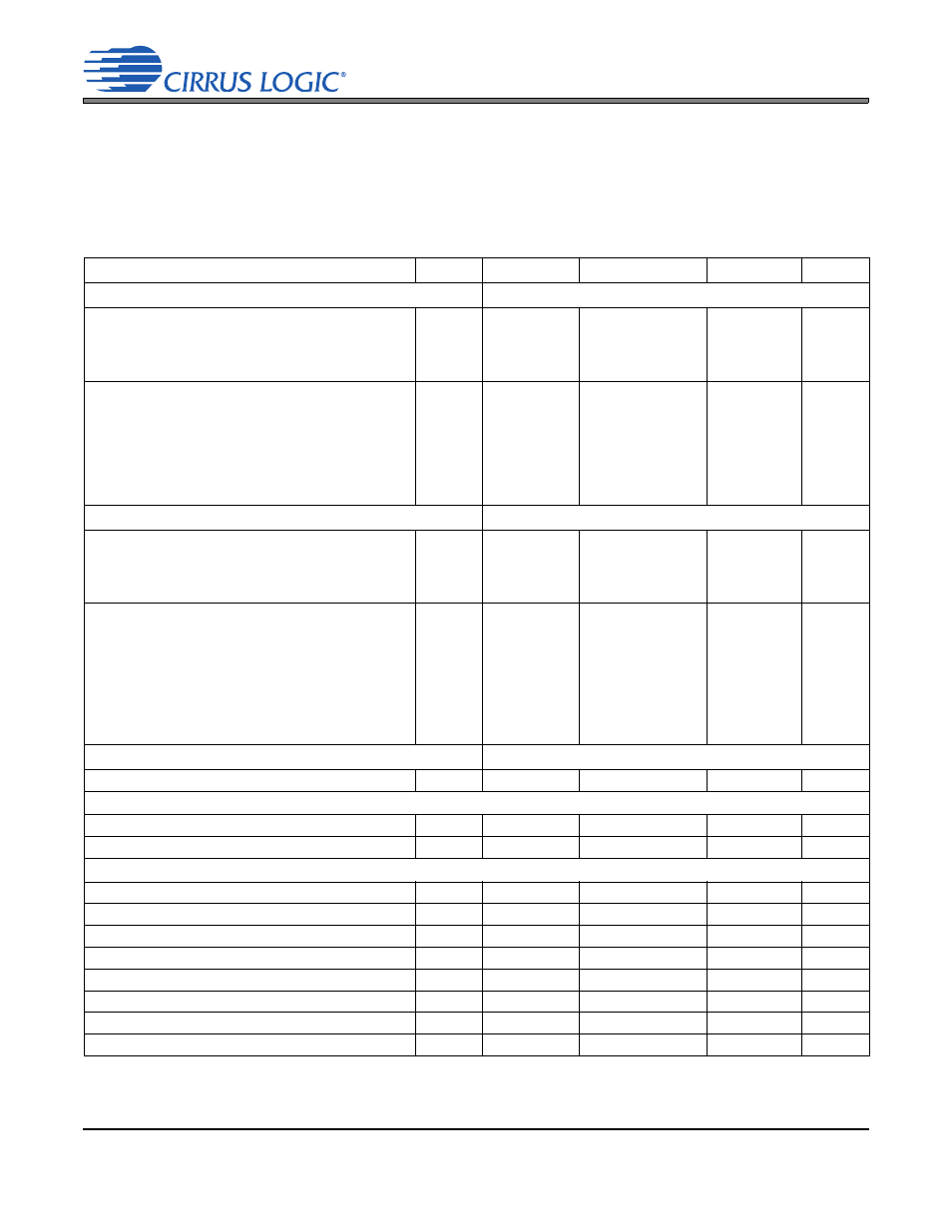
DAC Analog Characteristics - Commercial (-CZZ)
Test conditions (unless otherwise specified): VLS = VLC = 3.3 V; T
A
= 25° C; Input test signal is a 997 Hz
sine wave; Valid with the recommended capacitor values on VD_FILT, VQ, VBIAS (as shown in the typical
connection diagram in
) and output circuits as shown in
and
; Fs = 48 kHz,
96 kHz, and 192 kHz; measurement bandwidth 10 Hz to 20 kHz.
Notes: 3. One LSB of triangular PDF dither is added to data
4. R
L
and C
L
represent the minimum resistance and maximum capacitance required for the CS4350’s in-
ternal op-amp to remain stable. See
and
for more details.
Table 3. DAC Analog Characteristics - Commercial (-CZZ)
Parameter
Symbol
Min
Typ
Max
Unit
VA= 5.0 V
Single-ended/Differential
Dynamic Range
24-bit A-Weighted
unweighted
16-bit A-Weighted
unweighted
98/106
95/103
-
-
101/109
98/106
95/96
92/93
-
-
-
-
dB
dB
dB
dB
Total Harmonic Distortion + Noise
24-bit 0 dB
-20 dB
-60 dB
16-bit 0 dB
-20 dB
-60 dB
THD+N
-
-
-
-
-
-
-
-91
-78/-86
-38/-46
-90
-72/-73
-32/-33
-86/-87
-
-35/-43
-
-
-
dB
dB
dB
dB
dB
dB
VA= 3.3 V
Single-ended/Differential
Dynamic Range
24-bit A-Weighted
unweighted
16-bit A-Weighted
unweighted
98/106
95/103
-
-
101/109
98/106
95/96
92/93
-
-
-
-
dB
dB
dB
dB
Total Harmonic Distortion + Noise
24-bit 0 dB
-2 dB
-20 dB
-60 dB
16-bit 0 dB
-20 dB
-60 dB
THD+N
-
-
-
-
-
-
-
-86
-91/-93
-78/-86
-38/-46
-83
-72/-73
-32/-33
-77
-
-
-35/-43
-
-
-
dB
dB
dB
dB
dB
dB
dB
VA= 3.3 to 5.0 V
Interchannel Isolation
(1 kHz)
-
100
-
dB
DC Accuracy
Interchannel Gain Mismatch
-
0.1
0.25
dB
Gain Drift
-
-400
-
ppm/°C
Analog Output
Full Scale Output Voltage - Single Ended
2.61
2.78
2.96
Vpp
Full Scale Output Voltage - Differential
5.22
5.56
5.92
Vpp
Quiescent Voltage
V
Q
-
0.5•VA
-
VDC
Max DC Current draw from an AOUT pin
I
OUTmax
-
10
-
A
Max Current draw from VQ
I
Qmax
-
100
-
A
Max AC-Load Resistance
R
L
-
3
-
k
Max Load Capacitance
C
L
-
100
-
pF
Output Impedance
Z
OUT
-
100
-