Cs4350 – Cirrus Logic CS4350 User Manual
Page 12
12
DS691F2
CS4350
2.6
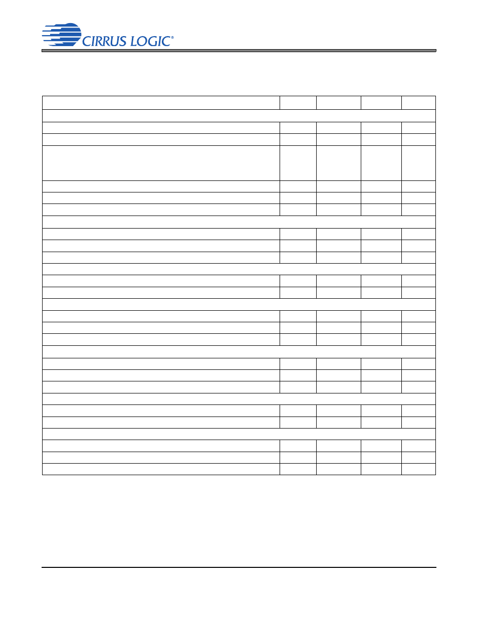
Switching Specifications - Serial Audio Interface
Inputs: Logic 0 = GND; Logic 1 = VLS; C
L
= 20 pF.
Note: 10. RMCK output frequency depends on the input LRCK frequency. See
for
more details.
Table 6. Switching Specifications - Serial Audio Interface
Parameters
Symbol Min
Max
Units
3.14 V
VA
5.25 V and 1.35 V
VLS
5.25 V
RMCK Output Frequency
7.680
55.3
MHz
RMCK Output Duty Cycle
45
55
%
Input Sample Rate
Single-Speed Mode
30
54
Double-Speed Mode
Fs
60
108
kHz
Quad-Speed Mode
120
216
LRCK Duty Cycle (Non-TDM Mode)
40
60
%
SDIN Setup Time Before SCLK Rising Edge
t
ds
1
-
ns
SDIN Hold Time After SCLK Rising Edge
t
dh
1
-
ns
4.75 V
VA
5.25 V and 3.14 V
VLS
5.25 V
SCLK Frequency
-
55.3
MHz
SCLK High Time
t
sckh
6
-
ns
SCLK Low Time
t
sckl
6
-
ns
Non-TDM Mode (refer to
)
LRCK Edge to SCLK Rising Edge
t
lcks
11
-
ns
SCLK Rising Edge to LRCK Edge
t
lckd
1
-
ns
TDM Mode (refer to
)
LRCK High Time
t
lrckh
6
-
ns
SCLK Rising to LRCK Falling Edge
t
fsh
3
-
ns
LRCK Rising Edge to SCLK Rising Edge
t
fss
1
-
ns
3.14 V
VA < 4.75 V or 1.35 V
VLS < 3.14 V
SCLK Frequency
-
27.7
MHz
SCLK High Time
t
sckh
11
-
ns
SCLK Low Time
t
sckl
11
-
ns
Non-TDM Mode (refer to
)
LRCK Edge to SCLK Rising Edge
t
lcks
16
-
ns
SCLK Rising Edge to LRCK Edge
t
lckd
1
-
ns
TDM Mode (refer to
)
LRCK High Time
t
lrckh
25
-
ns
SCLK Rising to LRCK Falling Edge
t
fsh
8
-
ns
LRCK Rising Edge to SCLK Rising Edge
t
fss
1
-
ns