Pin descriptions – Cirrus Logic CS42L55 User Manual
Page 8
8
DS773F1
CS42L55
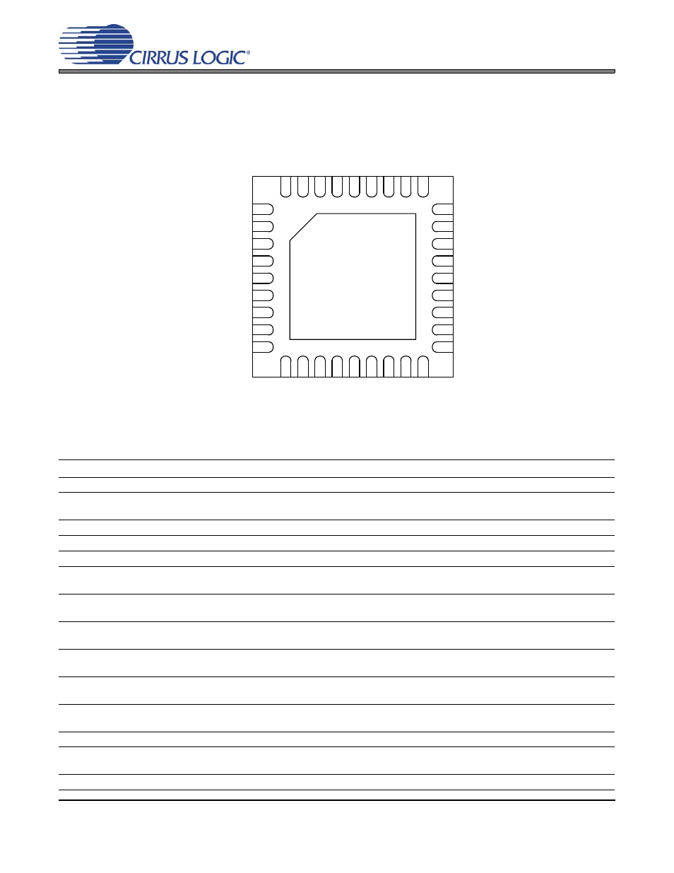
1. PIN DESCRIPTIONS
Pin Name
#
Pin Description
SDIN
1
Serial Audio Data Input (Input) - Input for two’s complement serial audio data.
LRCK
2
Left Right Clock (Input/Output) - Determines which channel, Left or Right, is currently active on the
serial audio data lines.
SDA
3
Serial Control Data (Input/Output) - Serial data for the I²C serial control port.
SCL
4
Serial Control Port Clock (Input) - Serial clock for the I²C serial control port.
VCP
5
Step-Down Charge Pump Power (Input) - Power supply for the step-down charge pump.
FLYP
6
Charge Pump Cap Positive Node (Output) - Positive node for the step-down charge pump’s flying
capacitor.
+VHPFILT
7
Step-Down Charge Pump Filter Connection (Output) - Power supply from the step-down charge
pump that provides the positive rail for the headphone and line amplifiers
FLYC
8
Charge Pump Cap Common Node (Output) - Common positive node for the step-down and inverting
charge pumps’ flying capacitors.
FLYN
9
Charge Pump Cap Negative Node (Output) - Negative node for the inverting charge pump’s flying
capacitor.
-VHPFILT
10
Inverting Charge Pump Filter Connection (Output) - Power supply from the inverting charge pump
that provides the negative rail for the headphone and line amplifiers.
HPOUTA
HPOUTB
11
13
Headphone Audio Output (Output) - The full-scale output level is specified in the HP Output Charac-
teristics specification table
HPREF
12
Pseudo Diff. Headphone Output Reference (Input) - Ground reference for the headphone amplifiers
LINEOUTA
LINEOUTB
14
16
Line Audio Output (Output) - The full-scale output level is specified in the Line Output Characteristics
specification table
LINEREF
15
Pseudo Diff. Line Output Reference (Input) - Ground reference for the line amplifiers.
8
7
6
3
1
9
2
4
5
10
11
12
13
14
15
18
17
16
19
26
20
21
22
23
24
25
27
35
28
29
30
31
32
33
34
36
VL
D
O
VDFILT
VL
MCLK
SD
OUT
HPO
U
TA
HPR
E
F
HPO
U
T
B
LINEOUTA
LINEREF
VA
LINEOUT
B
LRCK
SDA
SCL
FLYP
HPD
E
TECT
RESET
+VHPFILT
AIN2A
AIN2B
AFILTA
AFILTB
FILT+
VQ
AIN2REF
VCP
SDIN
AGND
SCLK
FLYN
AIN1A
AIN1REF
AIN1B
FLYC
Top-Down (Through Package)
View
-VHPFILT
GND/Thermal Pad