Cirrus Logic CS42L55 User Manual
Cs42l55, Digital to analog features, Analog to digital features
Copyright
© Cirrus Logic, Inc. 2007
(All Rights Reserved)
NOVEMBER '07
DS773F1
Ultra Low Power, Stereo CODEC w/Class H Headphone Amp
DIGITAL to ANALOG FEATURES
5 mW Stereo Playback Power Consumption
99 dB Dynamic Range (A-wtd)
-86 dB THD+N
Digital Signal Processing Engine
–
Bass & Treble Tone Control, De-Emphasis
–
Master Volume Control (+12 to -102 dB in
0.5 dB steps)
–
Soft-Ramp & Zero-Cross Transitions
–
Programmable Peak-Detect and Limiter
–
Beep Generator w/Full Tone Control
Stereo Headphone and Line Amplifiers
Step-Down/Inverting Charge Pump
Class H Amplifier - Automatic Supply Adj.
–
High Efficiency
–
Low EMI
Pseudo-Differential Ground-Centered Outputs
High HP Power Output at -75 dB THD+N
–
2 x 20 mW Into 32
Ω @1.8 V
–
2 x 20 mW Into 16
Ω @1.8 V
1 V
RMS
Line Output @1.8 V
Analog Vol. Ctl. (+12 to -55 dB in 1 dB steps)
Analog In to Analog Out Passthrough
Pop and Click Suppression
ANALOG to DIGITAL FEATURES
3.5 mW Stereo Record Power Consumption
95 dB Dynamic Range (A-wtd)
-87 dB THD+N
2:1 Stereo Input MUX
Analog Programmable Gain Amplifier (PGA)
(+12 to -6 dB in 0.5 dB steps)
+20 dB Boost
Programmable Automatic Level Control (ALC)
–
Noise Gate for Noise Suppression
–
Programmable Threshold &
Attack/Release Rates
Independent ADC Channel Control
Digital Vol. Ctl. (0 to -96 dB in 1 dB steps)
High-Pass Filter Disable for DC Measurements
Pseudo Differential Inputs
SYSTEM FEATURES
12 MHz USB Master Clock Input
Low Power Operation
–
Stereo Anlg. Passthrough: 3.3 mW @1.8 V
–
Stereo Rec. and Playback: 8.3 mW @1.8 V
Headphone Detect Input
(SYSTEM FEATURES continued on
)
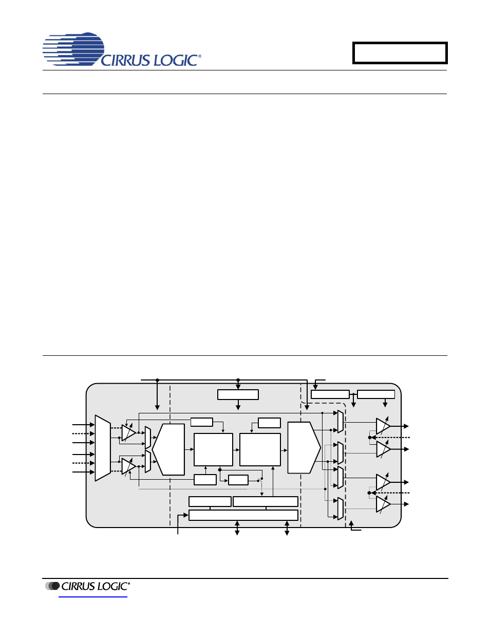
I²S Serial Audio
Input/Output
I
2
C Control
HPF
+1.65 V to +3.47 V
Interface Supply
Control Port
Serial Audio Port
Level Shifter
Multi-bit
ΔΣ ADC
Beep
+1.65 V to +2.71 V
Analog/Digital Supply
Multi-bit
ΔΣ ADC
ALC
ALC
Left HP
Output
Left 1
Pseudo Diff.
Input
Multi-bit
ΔΣ DAC
LDO Regulator
Ground-Centered
Amplifiers
Inverting
Mono mix,
Limiter, Bass,
Treble Adjust
Step-Down
Attenuator,
Boost, Mix
+VHP
-VHP
Right HP
Output
Left Line
Output
Right Line
Output
Left 2
Right 1
Right 2
Pseudo Diff.
Input
Pseudo Diff.
Input
Pseudo Diff.
Input
+1.65 V to +2.71 V
Charge Pump Supply
Headphone Detect
CS42L55
Document Outline
- 1. Pin Descriptions
- 2. Typical Connection Diagram
- 3. Characteristic and Specification Tables
- Recommended Operating Conditions
- Absolute Maximum Ratings
- Analog Input Characteristics
- ADC Digital Filter Characteristics
- HP Output Characteristics
- Line Output Characteristics
- Analog Passthrough Characteristics
- Combined DAC Interpolation & On-Chip Analog FIlter Response
- Switching Specifications - Serial Port
- Switching Specifications - Control Port
- Power Supply Rejection (PSRR) Characteristics
- Digital Interface Specifications & Characteristics
- Power Consumption - All Supplies = 1.8 V
- Power Consumption - All Supplies = 2.5 V
- 4. Applications
- 4.1 Overview
- 4.2 Analog Inputs
- 4.3 Analog In to Analog Out Passthrough
- 4.4 Analog Outputs
- 4.5 Class H Amplifier
- 4.6 Beep Generator
- 4.7 Limiter
- 4.8 Serial Port Clocking
- 4.9 Digital Interface Format
- 4.10 Initialization
- 4.11 Recommended DAC to HP or Line Power-Up Sequence (Playback)
- 4.12 Recommended PGA to HP or Line Power-Up Sequence (Analog Passthrough)
- 4.13 Required Initialization Settings
- 4.14 Control Port Operation
- 5. Register Quick Reference
- 6. Register Description
- 6.1 Fab I.D. and Revision Register (Address 01h) (Read Only)
- 6.2 Power Control 1 (Address 02h)
- 6.3 Power Control 2 (Address 03h)
- 6.4 Clocking Control 1 (Address 04h)
- 6.5 Clocking Control 2 (Address 05h)
- 6.6 Class H Power Control (Address 06h)
- 6.7 Miscellaneous Control (Address 07h)
- 6.8 ADC, Line, HP MUX (Address 08h)
- 6.9 HPF Control (Address 09h)
- 6.10 Misc. ADC Control (Address 0Ah)
- 6.11 PGA x MUX, Volume: PGA A (Address 0Bh) & PGA B (Address 0Ch)
- 6.12 ADCx Attenuator Control: ADCAATT (Address 0Dh) & ADCBATT (Address 0Eh)
- 6.13 Playback Control 1 (Address 0Fh)
- 6.14 ADCx Mixer Volume: ADCA (Address 10h) & ADCB (Address 11h)
- 6.15 PCMx Mixer Volume: PCMA (Address 12h) & PCMB (Address 13h)
- 6.16 Beep Frequency & On Time (Address 14h)
- 6.17 Beep Volume & Off Time (Address 15h)
- 6.18 Beep & Tone Configuration (Address 16h)
- 6.19 Tone Control (Address 17h)
- 6.20 Master Volume Control: MSTA (Address 18h) & MSTB (Address 19h)
- 6.21 Headphone Volume Control: HPA (Address 1Ah) & HPB (Address 1Bh)
- 6.22 Line Volume Control: LINEA (Address 1Ch) & LINEB (Address 1Dh)
- 6.23 Analog Input Advisory Volume (Address 1Eh)
- 6.24 Digital Input Advisory Volume (Address 1Fh)
- 6.25 ADC & PCM Channel Mixer (Address 20h)
- 6.26 Limiter Min/Max Thresholds (Address 21h)
- 6.27 Limiter Control, Release Rate (Address 22h)
- 6.28 Limiter Attack Rate (Address 23h)
- 6.29 ALC Enable & Attack Rate (Address 24h)
- 6.30 ALC Release Rate (Address 25h)
- 6.31 ALC Threshold (Address 26h)
- 6.32 Noise Gate Control (Address 27h)
- 6.33 ALC and Limiter Soft Ramp, Zero Cross Disables (Address 28h)
- 6.34 Status (Address 29h) (Read Only)
- 6.35 Charge Pump Frequency (Address 2Ah)
- 7. PCB Layout Considerations
- 8. Analog Volume Non-Linearity (DNL & INL)
- 9. ADC & DAC Digital Filters
- 10. Parameter Definitions
- 11. Package Dimensions
- 12. Ordering Information
- 13. References
- 14. Revision History