Cirrus Logic CDB42438 User Manual
Page 25
CDB42438
DS646DB2
25
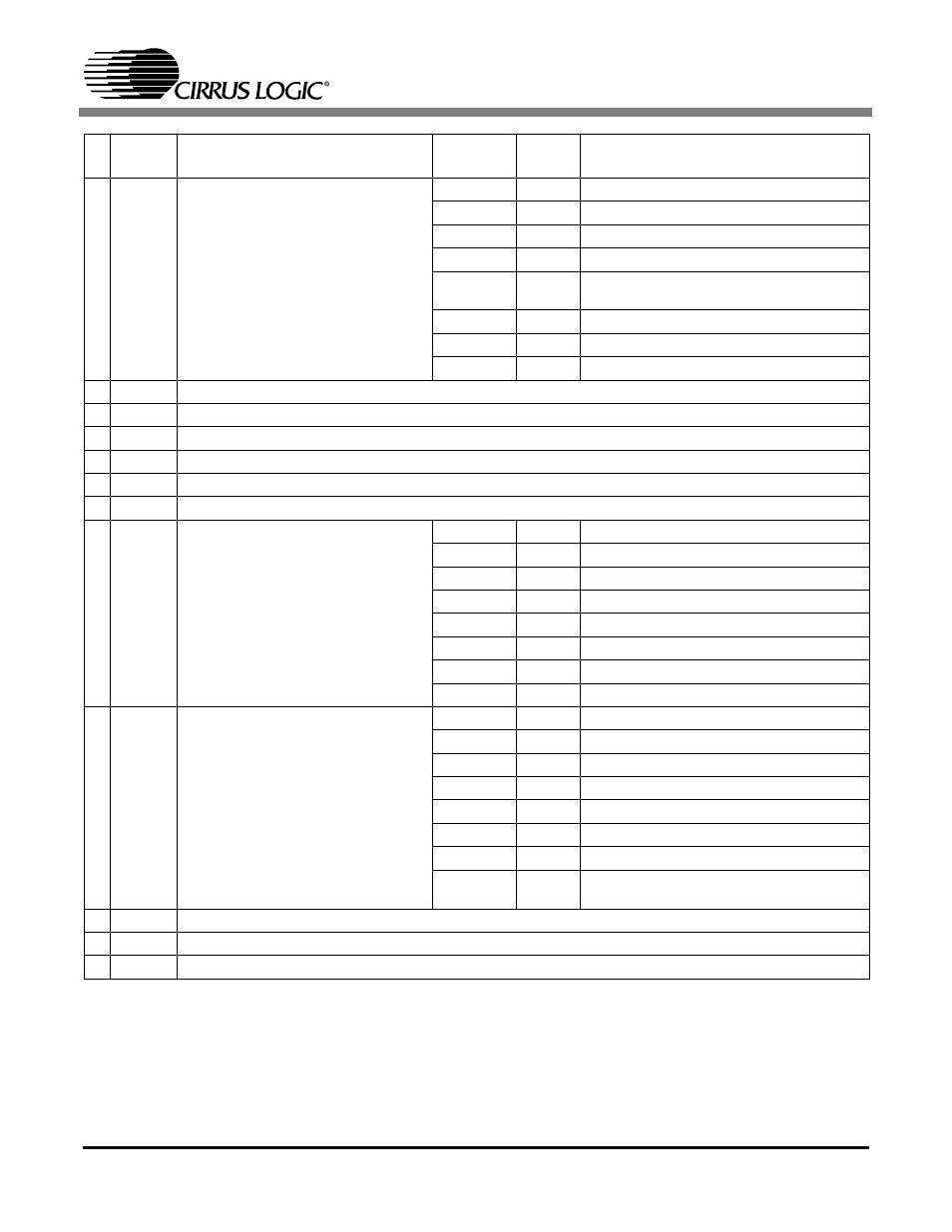
3
0011
TDMer w/CS8416 Data (S/PDIF4)
1) CS8416 Masters MCLK & PCM Subclocks
2) CS8416 data duplicated and Time-Division
Multiplexed into DAC_SDIN.
3) External ADC (AUX1-2) de-multiplexed
from ADC_SDOUT and input into CS8406.
01h
00h
TDM Conversion - CS8416 clocks & data to TDMer.
02h
03h
SDIN Control - TDMer output data input to SDIN.
03h
36h
CODEC Clock Control - CODEC slave to TDMer.
04h
79h
CS8406 Control - AUX to CS8406.
05h
38h
CS8416 Control - CS8416 masters MCLK bus and
provides PCM subclocks to the TDMer.
06h
EFh
Bypass Control - N/A.
07h
02h
DSP Header - DSP Slave to MCLK.
08h
41h
CS5341/Misc. Control - N/A.
4
0100
Reserved
5
0101
Reserved
6
0110
Reserved
7
0111
Reserved
8
1000
Reserved
9
1001
Reserved
10
1010
DSP Routing
1) DSP Masters MCLK & TDM Subclocks
(through FPGA).
01h
01h
TDM Conversion - TDMer powered down.
02h
01h
SDIN Control - DSP data input to DAC_SDIN.
03h
24h
CODEC Clock Control - CODEC slave to DSP.
04h
61h
CS8406 Control - N/A.
05h
29h
CS8416 Control - N/A.
06h
EFh
Bypass Control - N/A.
07h
07h
DSP Header Control - DSP Masters MCLK.
08h
41h
CS5341 Control - N/A.
11
1011
FPGA Bypass w/DSP MCLK
1) DSP Masters MCLK & TDM Subclocks
(bypassing FPGA).
01h
F0h
TDM Conversion - N/A.
02h
00h
SDIN Control - N/A.
03h
09h
CODEC Clock Control - N/A.
04h
01h
CS8406 Control - N/A.
05h
29h
CS8416 Control - N/A.
06h
0Ch
Bypass Control - DSP to CODEC.
07h
07h
Misc. Control - DSP Master.
08h
41h
CS5341 Control - Left-justified data from CS5341.
Maximum MCLK = 25 MHz.
12
1100
Reserved
13
1101
Reserved
14
1110
Reserved
SW[3:0]
General Description
Register
Address
Value
Detail Description