Fpga register description, 1 tdm conversion (address 01h), 2 codec sdin control (address 02h) – Cirrus Logic CDB42438 User Manual
Page 16: Table 1. data to sdin, P 16
CDB42438
16
DS646DB2
5. FPGA REGISTER DESCRIPTION
All registers are read/write. See the following bit definition tables for bit assignment information. The de-
fault state of each bit after a power-up sequence or reset is listed in each bit description.
5.1
TDM CONVERSION (ADDRESS 01H)
5.1.1
PCM2TDM CLOCK SELECTION (DSP/CS8416)
Default = 0
0 - CS8416
1- DSP Header
Function:
This bit selects the clock source for the PCM2TDM (P2T) converter. It also selects the data source
for Slot 1-4 (see Figure 5 on page 12) of the TDMer.
5.1.2
POWER DOWN TDM CONVERTER (PDN_TDMER)
Default = 0
0 - Disabled
1- Enabled
Function:
This bit powers down the TDMer.
5.2
CODEC SDIN CONTROL (ADDRESS 02H)
5.2.1
SDIN MUX(SDIN.MUX)
Default = 10
Function:
This MUX selects the data lines from the DSP Header, the ADC and the TDM Stream from the TDMer
(see Figure 4 on page 11).
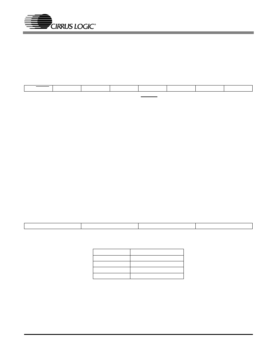
7
6
5
4
3
2
1
0
DSP/CS8416
Reserved
Reserved
Reserved
Reserved
Reserved
Reserved
PDN_TDMer
7
6
5
4
3
2
1
0
Reserved
Reserved
Reserved
Reserved
Reserved
Reserved
SDIN.MUX1
SDIN.MUX0
SDIN.MUX[1:0]
Data Selection
00
Reserved
01
DSP_DOUT
10
ADC_SDOUT
11
TDM Stream
Table 1. Data to SDIN