Cirrus Logic CDB42438 User Manual
Features, Description, Cs8406 s/pdif digital audio transmitter
Copyright
© Cirrus Logic, Inc. 2004
(All Rights Reserved)
Cirrus Logic, Inc.
www.cirrus.com
CDB42438
Evaluation Board For CS42438
Features
z
Single-ended/Single-ended to Differential
Analog Inputs
z
Single-ended/Differential to Single-ended
Analog Outputs
z
CS8406 S/PDIF Digital Audio Transmitter
z
CS8416 S/PDIF Digital Audio Receiver
z
Header for Optional External Software
Configuration of CS42438
z
Header for External DSP Serial Audio I/O
z
3.3 V Logic Interface
z
Pre-defined Software Scripts
z
S/PDIF-to-TDM Conversion for Easy
Evaluation of the TDM Digital Interface
z
Demonstrates Recommended Layout and
Grounding Arrangements
z
Windows
®
Compatible Software Interface to
Configure CS42438 and Inter-board
Connections
ORDERING INFORMATION
CDB42438
Evaluation Board
Description
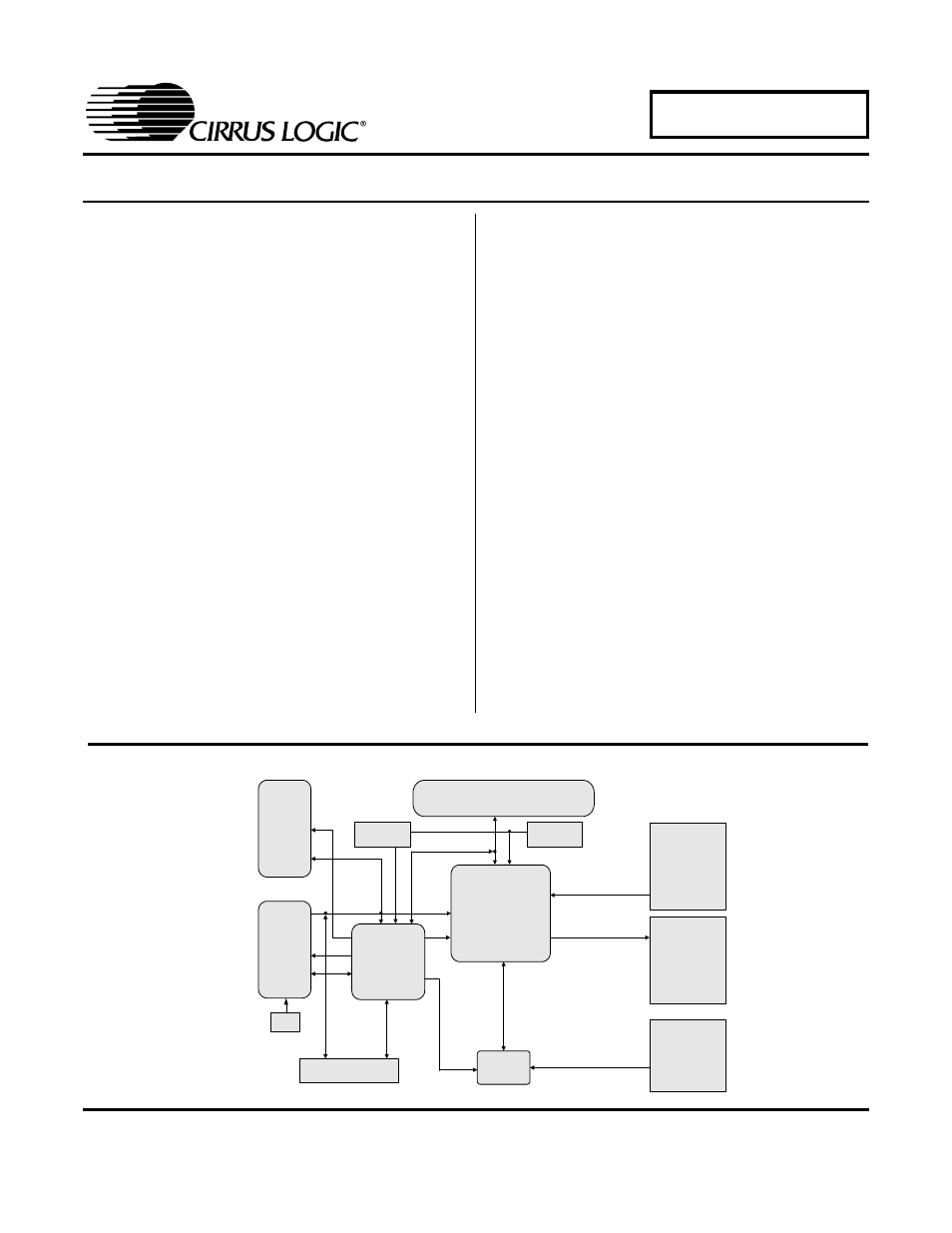
The CDB42438 evaluation board is an excellent means
for evaluating the CS42438 CODEC. Evaluation re-
quires an analog/digital signal source and analyzer, and
power supplies. Optionally, a Windows
®
PC compatible
computer may be used to evaluate the CS42438 in soft-
ware mode.
System timing can be provided by the CS8416, or by a
DSP I/O stake header with a DSP connected. System
timing for TDM mode is provided by an FPGA using
clocks derived from the CS8416 or DSP I/O header.
RCA phono jacks are provided for the CS42438 analog
inputs and outputs. Digital data I/O is available via RCA
phono or optical connectors to the CS8416 and CS8406.
6 pre-defined board setup options are selectable using a
6-position DIP switch.
The Windows
®
software provides a GUI to make config-
uration of the CDB42438 easy. The software
communicates through the PC’s serial port to configure
the control port registers so that all features of the
CS42438 can be evaluated. The evaluation board may
also be configured to accept external timing and data
signals for operation in a user application during system
development.
I
CS42438
CS8416
S/PDIF
Input
y Differential to
Single-Ended
Output
y Single-Ended
Output
y Single-Ended to
Differential Input
y Single-Ended
Input
Serial Control Port
FPGA
CS8406
S/PDIF
Output
DSP HEADER
CS5341
Osc.
ANALOG INPUT
ANALOG OUTPUT
y Single-Ended
Input
AUXILIARY
ANALOG INPUT
MCLK Divided
Clocks
/Data
Hardware
Setup
MCLK BUS
A
D
C/DA
C
Cl
oc
k
s
&
Data
ADC/DAC
Clocks/
Data
Cl
oc
k
s
/Data
I
2
C/SPI Header
H/W Switches
OCT ‘04
DS646DB2
Document Outline
- Features & Description
- Table of Contents
- List of Figures
- List of Tables
- 1. System Overview
- 2. Software Mode
- 3. FPGA System Overview
- 4. FPGA Register Quick Reference
- 5. FPGA Register Description
- 5.1 TDM Conversion (address 01h)
- 5.2 CODEC SDIN Control (address 02h)
- Table 1. Data to SDIN
- 5.3 CODEC Clock Control (address 03h)
- Table 2. Clocks toCODEC
- 5.4 CS8406 Control (address 04h)
- Table 3. Data to CS8406
- 5.5 CS8416 Control (address 05h)
- 5.6 Bypass Control (address 06h)
- 5.7 DSP Header Control (address 07h)
- Table 4. Data to DSP
- 5.8 CS5341 and Miscellaneous Control (Address 08h)
- 6. Hardware Mode
- 7. CDB Connectors and Jumpers
- 8. CDB Block Diagram
- 9. CDB Schematics
- Figure 8. CS42438
- Figure 9. DSP Header
- Figure 10. S/PDIF Input
- Figure 11. S/PDIF Output
- Figure 12. FPGA
- Figure 13. FPGA Connections
- Figure 14. Control Port
- Figure 15. Control Port Connections
- Figure 16. Analog Input 1-2
- Figure 17. Analog Input 3-4
- Figure 18. Analog Input 5
- Figure 19. Analog Input 6
- Figure 20. Analog Input 7-8
- Figure 21. Analog Output 1-2
- Figure 22. Analog Output 3-4
- Figure 23. Analog Output 5-6
- Figure 24. Analog Output 7-8
- Figure 25. Power
- 10. CDB LAYOUT
- 11. Revision History