Internal sub-clock routing, Figure 3. internal sub-clock routing, Sections 3.2 to 3.4 show graphical descriptions – Cirrus Logic CDB42438 User Manual
Page 10
CDB42438
10
DS646DB2
3.2.
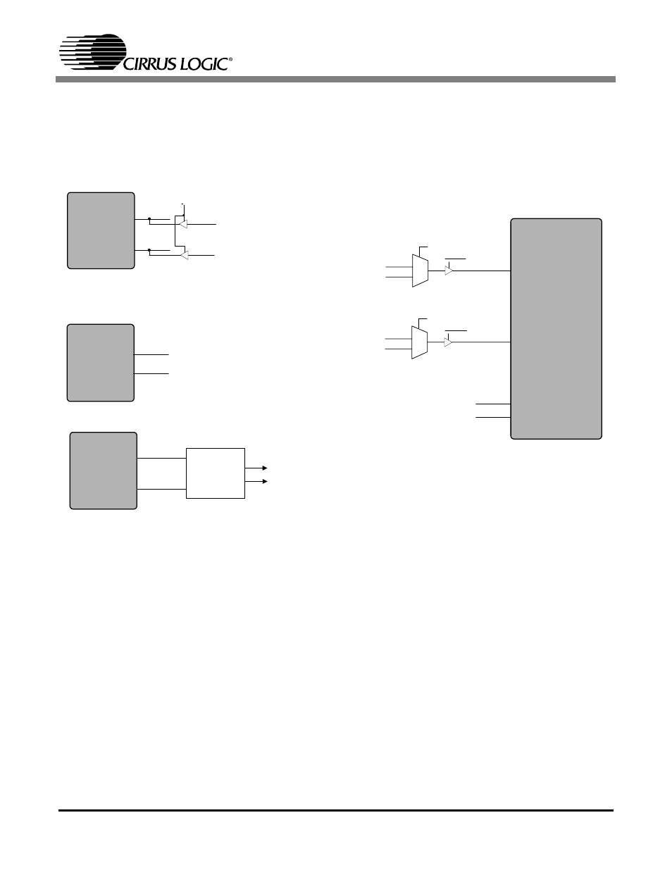
Internal Sub-Clock Routing
The graphical description below shows the internal clock routing topology between the CS42438,
CS8416, CS8406 and DSP Header. Refer to registers “CODEC Clock Control (address 03h)” on
page 17, “CS8406 Control (address 04h)” on page 17 and “CS8416 Control (address 05h)” on
page 18 for configuration settings.
CS8416
DSP Header
LRCK
CS8406
CS42438
FS
SCLK
AUX_LRCK
AUX_SCLK
SCLK
DSP FS
DSP SCLK
LRCK
SCLK
DSP_FS
FS
CODEC_CLK.MUX[1:0]
AUX LRCK
AUX SCLK
CS8416 LRCK
CS8416 SCLK
DSP_FS
DSP_SCLK
AUX LRCK
AUX SCLK
TDMer
M/S
FPGA->CODEC
FS
256Fs
256Fs
CODEC_CLK.MUX[1:0]
FPGA->CODEC
DSP_SCLK
Figure 3. Internal Sub-Clock Routing
See also other documents in the category Cirrus Logic Hardware:
- CobraNet (147 pages)
- CS4961xx (54 pages)
- CS150x (8 pages)
- CS1501 (16 pages)
- CS1601 (2 pages)
- CS1601 (16 pages)
- CS1610 (16 pages)
- CRD1610-8W (24 pages)
- CRD1611-8W (25 pages)
- CDB1610-8W (21 pages)
- CS1610A (18 pages)
- CDB1611-8W (21 pages)
- CDB1610A-8W (21 pages)
- CDB1611A-8W (21 pages)
- CRD1610A-8W (24 pages)
- CRD1611A-8W (25 pages)
- CS1615 (16 pages)
- AN403 (15 pages)
- AN401 (14 pages)
- AN400 (15 pages)
- AN375 (27 pages)
- AN376 (9 pages)
- CRD1615-8W (22 pages)
- CRD1616-8W (23 pages)
- AN402 (14 pages)
- AN404 (15 pages)
- CRD1615A-8W (21 pages)
- CS1615A (16 pages)
- CS1630 (56 pages)
- AN374 (35 pages)
- AN368 (80 pages)
- CRD1630-10W (24 pages)
- CRD1631-10W (25 pages)
- CS1680 (16 pages)
- AN405 (13 pages)
- AN379 (31 pages)
- CRD1680-7W (31 pages)
- AN335 (10 pages)
- AN334 (6 pages)
- AN312 (14 pages)
- AN Integrating CobraNet into Audio Products (16 pages)
- CobraNet Audio Routing Primer (9 pages)
- Bundle Assignments in CobraNet Systems (3 pages)
- CS2300-01 (3 pages)
- CS2000-CP (38 pages)