5 external mclk control, 1 cs5341 mclk, 2 tdmer mclk – Cirrus Logic CDB42438 User Manual
Page 13: Figure 6. external mclk control, 1 cs5341 mclk 3.5.2 tdmer mclk, Section 3.5 shows the graphical
CDB42438
DS646DB2
13
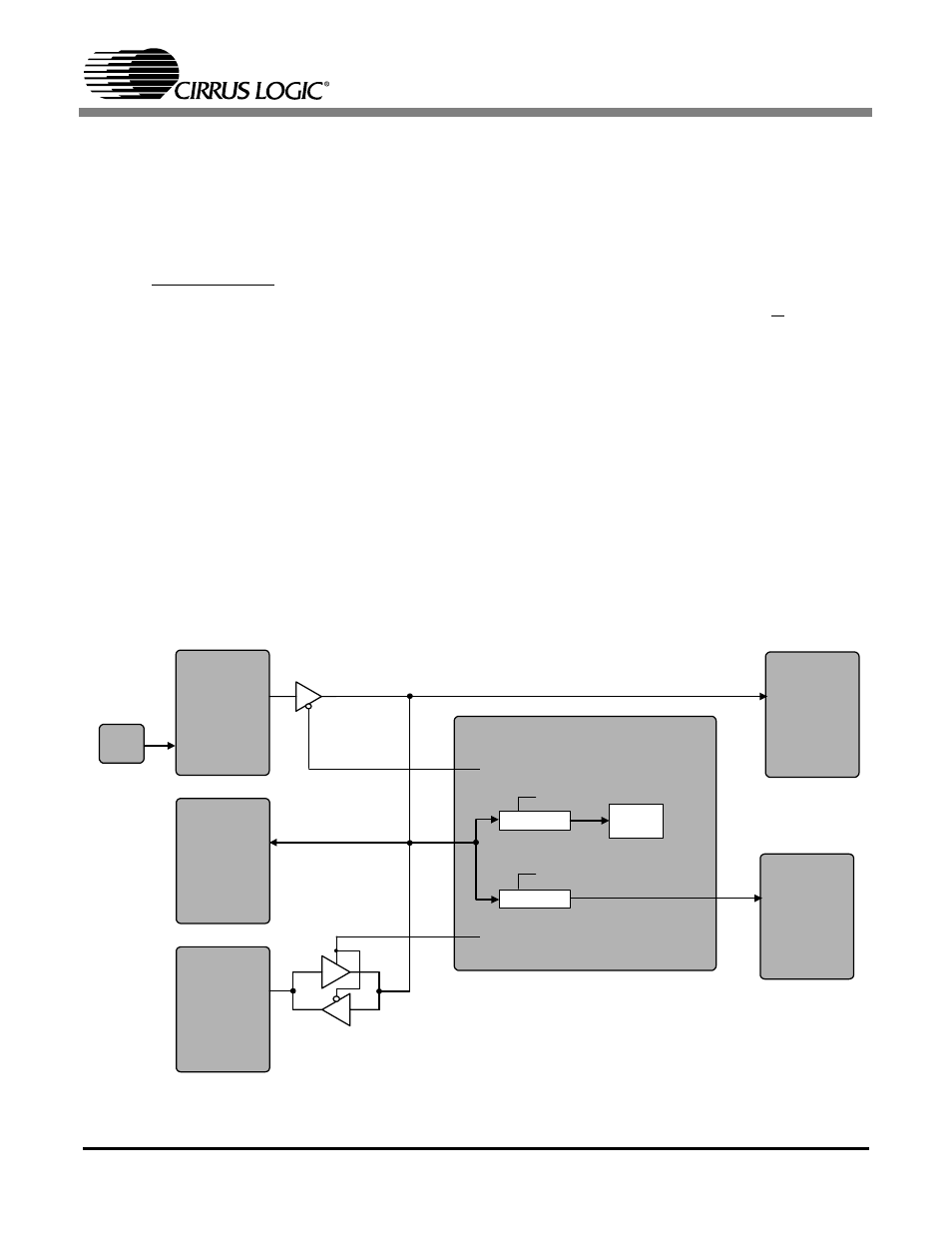
3.5
External MCLK Control
Several sources for MCLK exist on the CDB42438. The crystal oscillator, Y1, will master the
MCLK bus when no S/PDIF signal is input to the CS8416 (refer to the CS8416 data sheet for
details on OMCK operation). This signal will be driven directly out the CS8416.
The CS8416 will generate a master clock whenever its internal PLL is locked to the incoming
S/PDIF stream. This MCLK signal from the CS8416 can be taken off the MCLK bus by setting
the “RMCK_Master” bit in the register “CS8416 Control (address 05h)” on page 18.
The DSP Header can master or slave the MCLK bus by setting the “MCLK_M/S” bit in the
register “DSP Header Control (address 07h)” on page 20 accordingly.
3.5.1
CS5341 MCLK
To accommodate an MCLK signal greater than 25 MHz on the MCLK bus, a 2.0 divider
internal to the FPGA has been implemented. The divided MCLK signal is routed only to
the CS5341. Refer to register “CS5341 and Miscellaneous Control (Address 08h)” on
page 22 for the required setting.
3.5.2
TDMer MCLK
MCLK signals greater than 256Fs must be divided accordingly to maintain a 256Fs MCLK
signal into the TDMer. A 1.5 and a 2.0 divider has been implemented inside the FPGA.
Refer to register “CS5341 and Miscellaneous Control (Address 08h)” on page 22 for the
required setting.
CS8416
CS8406
DSP Header
FPGA
RMCK
OMCK
OSC
OMCK
DSP_MCLK
CS42438
MCLK
CS5341
MCLK
Divider
Divider
TDMer
Reg 08h[6:5]
Reg 08h[3:2]
MCLK_M/S
Reg 07h[0]
RMCK_Master
Reg 05h[0]
Figure 6. External MCLK Control