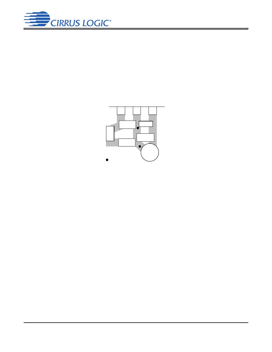
3 circuit board layout, Figure 26. recommended layout example – Cirrus Logic CS42428 User Manual
Page 63

DS605F2
63
CS42428
9.1.3
Circuit Board Layout
Board layout and capacitor choice affect each other and determine the performance of the PLL. Figure
26 illustrates a suggested layout for the PLL filter components and for bypassing the analog supply volt-
age. The 10 µF bypass capacitor is an electrolytic in a surface-mount case A or thru-hole package. RFILT,
CFILT, CRIP, and the 0.1 µF decoupling capacitor are in an 0805 form factor. The 0.01 µF decoupling
capacitor is in the 0603 form factor. The traces are on the top surface of the board with the IC so that there
is no via inductance. The traces themselves are short to minimize the inductance in the filter path. The
VA and AGND traces extend back to their origin and are shown only in truncated form in the drawing.
VA
AG
ND
LP
FL
T
CFILT
RFI
L
T
CRIP
0.1 µF
0.01 µF
10 µF
= via to ground plane
Figure 26. Recommended Layout Example
- CobraNet (147 pages)
- CS4961xx (54 pages)
- CS150x (8 pages)
- CS1501 (16 pages)
- CS1601 (2 pages)
- CS1601 (16 pages)
- CS1610 (16 pages)
- CRD1610-8W (24 pages)
- CRD1611-8W (25 pages)
- CDB1610-8W (21 pages)
- CS1610A (18 pages)
- CDB1611-8W (21 pages)
- CDB1610A-8W (21 pages)
- CDB1611A-8W (21 pages)
- CRD1610A-8W (24 pages)
- CRD1611A-8W (25 pages)
- CS1615 (16 pages)
- AN403 (15 pages)
- AN401 (14 pages)
- AN400 (15 pages)
- AN375 (27 pages)
- AN376 (9 pages)
- CRD1615-8W (22 pages)
- CRD1616-8W (23 pages)
- AN402 (14 pages)
- AN404 (15 pages)
- CRD1615A-8W (21 pages)
- CS1615A (16 pages)
- CS1630 (56 pages)
- AN374 (35 pages)
- AN368 (80 pages)
- CRD1630-10W (24 pages)
- CRD1631-10W (25 pages)
- CS1680 (16 pages)
- AN405 (13 pages)
- AN379 (31 pages)
- CRD1680-7W (31 pages)
- AN335 (10 pages)
- AN334 (6 pages)
- AN312 (14 pages)
- AN Integrating CobraNet into Audio Products (16 pages)
- CobraNet Audio Routing Primer (9 pages)
- Bundle Assignments in CobraNet Systems (3 pages)
- CS2300-01 (3 pages)
- CS2000-CP (38 pages)
