An379, And to the load after fet q, Turns off. capacitance c – Cirrus Logic AN379 User Manual
Page 8: Drain voltage and current, and catch diode d, Current, Figure 3. buck converter, Figure 4a. fet drain voltage, Cs1680
AN379
8
AN379REV2
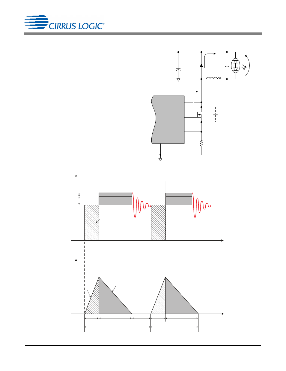
The Buck Topology
Figure 3 illustrates a typical implementation of a buck
converter using the CS1680 controller. The load is
composed of a string of LEDs. Diode D
BUCK
is the
catch diode, also known as the freewheeling diode,
and its function is to allow the current to flow in
inductor L
BUCK
and to the load after FET Q
BUCK
turns
off. Capacitance C
P
represents the combined
parasitic capacitance associated with the FET drain
node, usually consisting of the FET drain-source
capacitance, inductor winding capacitance, and
diode D
BUCK
reverse bias capacitance. For a non-
tapped buck topology the leakage inductance L
K
is
not a concern.
The buck stage is supplied by the boost output
voltage. The boost output voltage is regulated within
15% by the boost stage. The buck control loop
regulates the output current as long as the peak
current has sufficient margin to rise 10% at the lowest
boost output voltage. Figure 4a and Figure 4b
illustrate idealized waveforms of the buck power FET
Q
BUCK
drain voltage and current, and catch diode
D
BUCK
current.
LED+
LED-
C
OUT
R
BUCK(Sense)
Q
BUCK
GND
BUCKGD
BUCKSENSE
CS1680
V
BST
D
BUCK
I1
V
OUT
C
P
I2
BUCKZCD
C2
C
BST
L
BUCK
Figure 3. Buck Converter
Area =
V
Diode
ު T2
BUCK
Area = V
OUT
ު T2
BUCK
Area = (V
BST
- V
OUT
)
ު T1
BUCK
V
BST
V
Diode
V
OUT
t
V
BST
- V
OUT
Figure 4a. FET Drain Voltage
T1
BUCK
TT
BUCK
T3
BUCK
'
C
1-
'
C
T2
BUCK
1
t
I
BUCKPK
I1
I2
Figure 4b. Current Through Buck Power FET and Catch Diode