3 buck stage design, An379 – Cirrus Logic AN379 User Manual
Page 7
AN379
AN379REV2
7
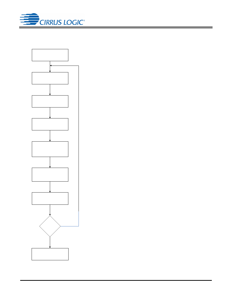
3.3 Buck Stage Design
Figure 2 illustrates the steps for designing the buck stage.
Figure 2. Buck Stage Design
Buck Specification
Determine V
BST
,
V
Breakdown
, and V
Margin
Define GAIN
TT
and
(T1
BUCK
+ T2
BUCK
)
Calculate
Duty Cycle
C
and
Inductance L
BUCK
Calculate TT
BUCK
and
C
Fit?
Yes
No
Calculate I
BUCKPK
,
R
BUCK(Sense)
, and T3
BUCK
Calculate RMS Current
and Output Capacitor
Buck Inductor
Specification
Steps for the Buck Design
1. Set the boost output voltage V
BST
.
2. Determine the FET breakdown voltage V
Breakdown
and
margin voltage V
Margin
.
3. Select a FET that aligns with the quality standards of the
designer’s company.
4. Determine critical period (T1
BUCK
+T2
BUCK
).
5. Define gain factor GAIN
TT
.
6. Calculate time T3
BUCK
using fixed gain factor GAIN
TT
.
7. Calculate peak current I
BUCKPK
using gain factor GAIN
TT
.
8. Calculate sense resistor R
BUCK(Sense)
using peak
current I
BUCKPK
.
9. Using maximum voltages V
BST
and V
OUT
determine the
critical duty cycle
C
.
10. Calculate maximum periods T1
BUCK
and T2
BUCK
.
11. Calculate buck inductance L
BUCK
using time T1
BUCK
.
12. Calculate RMS current in buck inductor L
BUCK
using peak
current I
BUCKPK
and duty cycle.
13. Determine the buck inductor specifications.
14. Select an output capacitor.
15. Determine if the buck inductor fits into a specified form
factor after designing and constructing the buck inductor.
Repeat steps 4 to 13 until form factor criteria is met.
16. Refine the circuit with the final buck inductor design.
17. Validate that the system meets the operating criteria.