1 operating parameters, 2 overview of design steps, An379 – Cirrus Logic AN379 User Manual
Page 6
AN379
6
AN379REV2
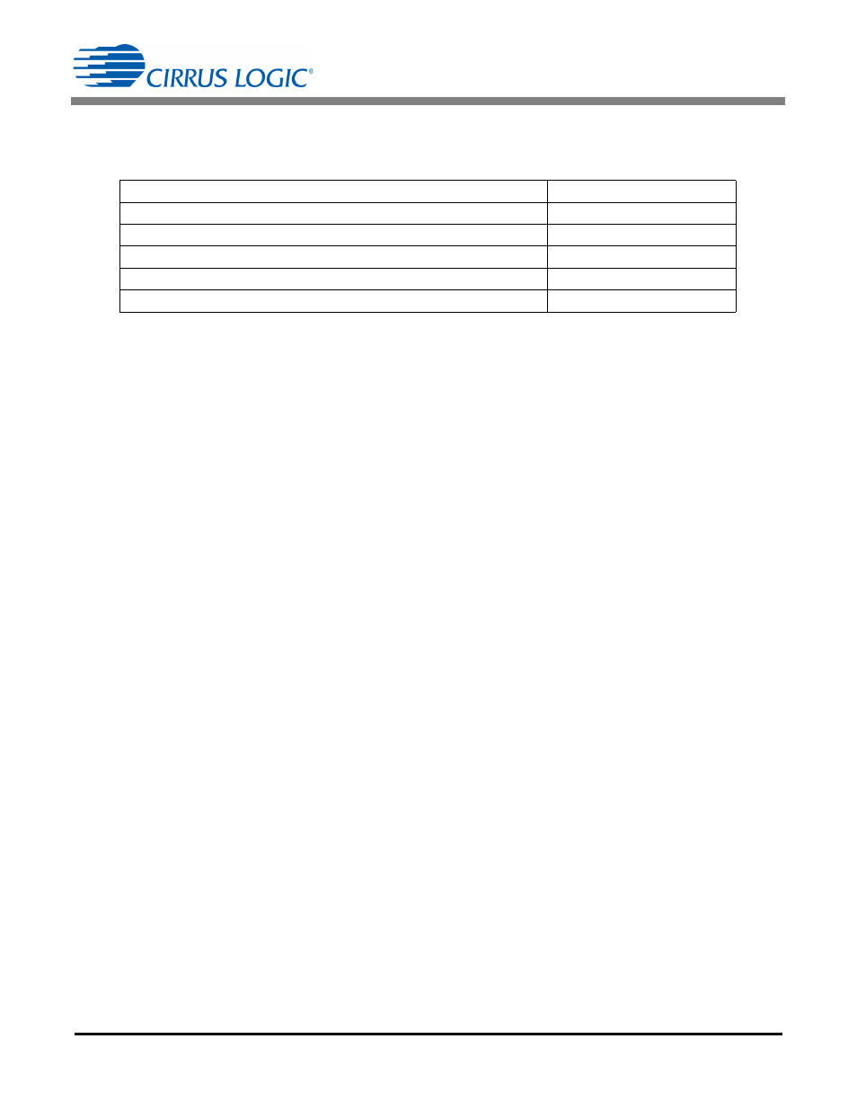
3.1 Operating Parameters
To initiate the design procedure, a set of operating parameters is required. Operating parameters required for
the analytical process are outlined in the table below.
Parameters critical to the overall design, but not specifically addressed in this document, include efficiency,
form factor, layout, and operating temperature
3.2 Overview of Design Steps
The CS1680 LED driver IC controls a power converter system that has two distinct power-conversion stages.
The IC requires supporting circuitry to provide a steady-state power supply with startup, and a clamp circuit.
The recommended design process is outlined below:
1. Start with the buck stage.
2. Design for full power at maximum boost output voltage V
BST
. Note that any design may require different
operating parameters to be turned off during a design procedure.
3. Optimize the buck stage through validation and design iteration.
4. Base the boost stage design on the power requirement of the buck stage.
5. Start the boost stage design in Mode3.
6. Determine peak current I
BSTPK
in the boost inductor.
7. Calculate boost sense resistor R
BST(Sense)
and resistor R
CTRL1
.
8. Determine boost inductance L
BST
. Consider the impact on the ripple current.
9. Design for boost peak current in Mode2 by determining resistor R
CTRL2
.
10. Select the boost inductor. Take into account that a large boost inductance value minimizes ripple current
but tends to have an adverse impact on form factor for a given saturation current.
11. Select the boost input and output capacitors.
12. Pick the boost FET based on peak current ratings.
13. Determine the clamp circuit.
14. Choose the power supply components.
15. Complete the non-power-converting circuitry: ZCD, BOP, eOTP, startup circuit.
16. Lay out the PCB.
The buck stage design is carried out at the full brightness (full load) point. To achieve an optimal solution,
several iterations of the design process may be required.
Parameters
Symbol
Output Power
P
OUT
AC Input Voltage
V
IN
Output Voltage
V
OUT
Load Current
I
OUT
Maximum Buck Switching Frequency
*
F
BUCKSW(max)
* Increasing the switching frequency may reduce the size of the magnetics but increase switching losses in the
FET and transformer.