4 design example, 1 buck design steps, Step 1) select a value for boost output voltage – Cirrus Logic AN379 User Manual
Page 21: Step 2) select an appropriate fet, An379
AN379
AN379REV2
21
4 Design Example
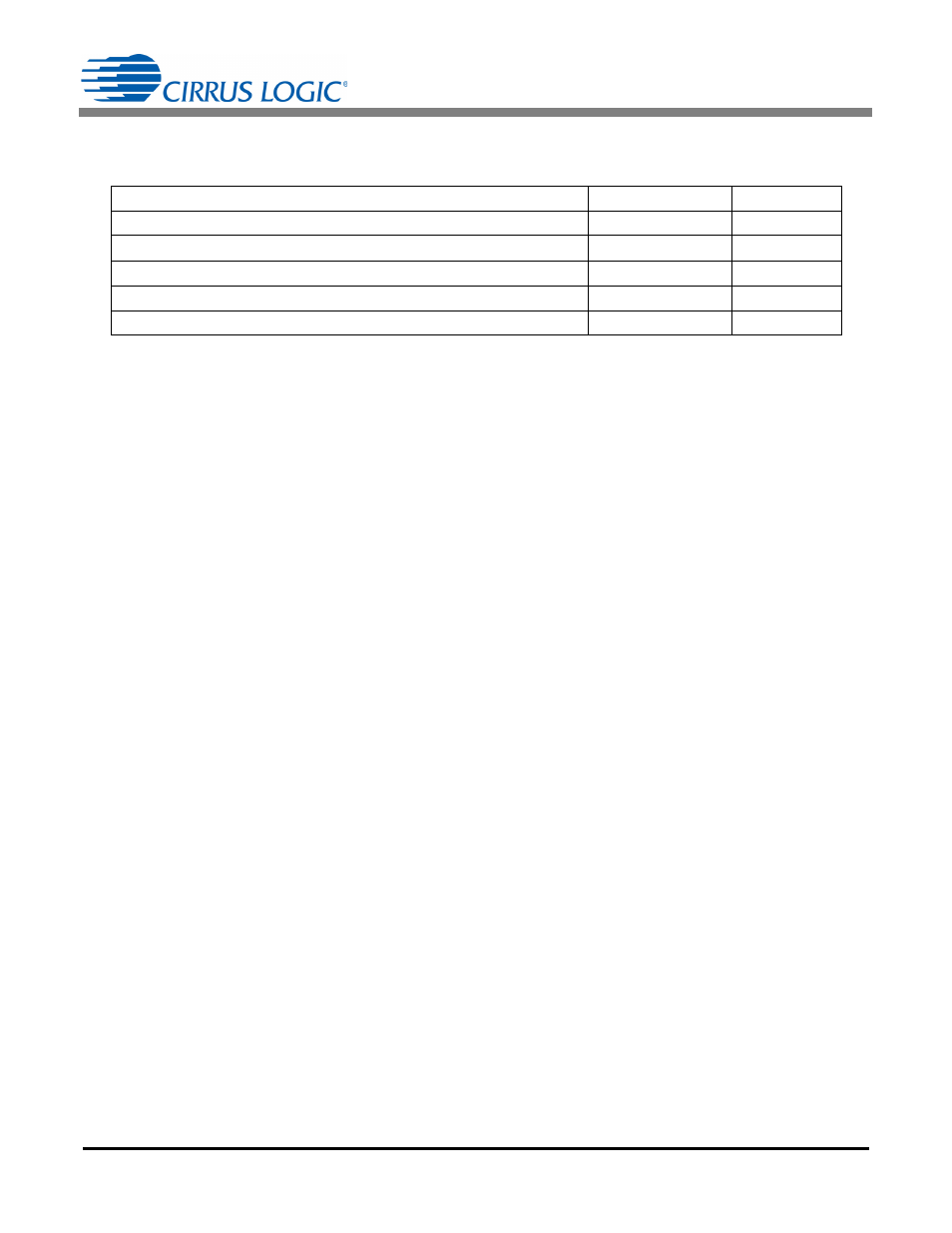
The required operating parameters for the analytical process are outlined in the table below.
Notes:
1. It is desirable to use a power FET that does not exceed 50V breakdown.
2. System efficiency estimate is 77%
3. Rectifying Schottky diode voltage V
F
is equal to 0.5V
4.1 Buck Design Steps
The example design is a 12VAC application. A maximum buck switching frequency of 150kHz is selected,
which corresponds to a switching period TT
BUCK
of 6.67µs.
Step 1) Select a Value for Boost Output Voltage
Full-scale boost output voltage V
BST(full)
is determined by sense resistor R
BST
which is set to 604k
. Use
Equation 7 on page 10 to calculate the full scale boost output voltage V
BST(full)
. Solve Equation 40 for boost
voltage V
BST(full)
:
For a 12VAC system, full-scale voltage V
BST(full)
is approximately 40V. The nominal boost output voltage V
BST
is 28V and droops to its lowest value towards the end of each half line-cycle until the boosting process starts
again in the next half line-cycle. The CS1680 limits the boost output voltage to ±15%. Therefore, minimum
boost output voltage V
BST(min)
and maximum boost output voltage V
BST(max)
are calculated using Equation 41
and 42, respectively:
Step 2) Select an Appropriate FET
Buck converters have an optimal operating range above 50% duty cycle, although any duty cycle above 30%
is close to optimal. When FET Q
BUCK
is turned off, the maximum drain voltage V
Drain(max)
occurs and is
calculated from Equation 43:
Use Equation 9 on page 11 to determine FET breakdown voltage V
Breakdown
. Solve Equation 44 for
voltage V
Breakdown
:
Parameters
Symbol
Value
Output Power
P
OUT
5.15W
AC Input Voltage
V
IN
12 VAC
10%
Output Voltage
V
OUT
12V
10%
Load Current
I
OUT
430 mA
Maximum Buck Switching Frequency
*
F
BUCKSW(max)
150 kHz
* Increasing the switching frequency may reduce the size of the magnetics but increase switching losses in the FET
and inductor.
V
BST full
I
ref
R
BST
20k
+
64
A
604k
20k
+
39.9V
=
=
=
[Eq. 40]
V
BST min
28V
=
0.85
24V
=
[Eq. 41]
V
BST max
28V
=
1.15
32V
=
[Eq. 42]
V
Drain max
V
BST BOP
V
Diode
+
40V 0.9375
0.5V
+
38V
=
=
=
[Eq. 43]
V
Breakdown
V
BST BOP
V
Diode
V
M
in
arg
+
+
37.5V 0.5V V
M
in
arg
+
+
=
=
[Eq. 44]