3 design process, An379 – Cirrus Logic AN379 User Manual
Page 5
AN379
AN379REV2
5
3 Design Process
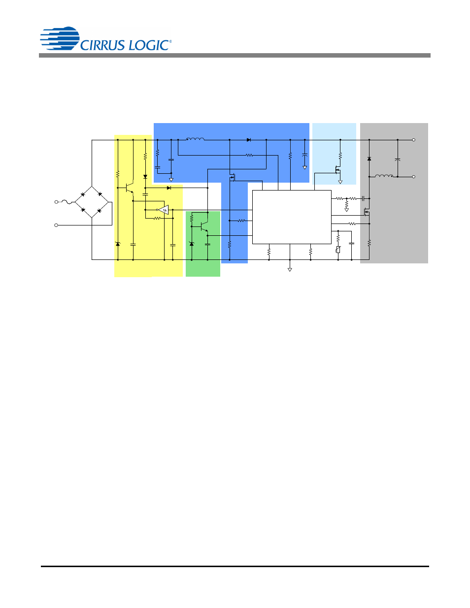
The design process for a two-stage power converter system can be partitioned into five circuit blocks (see Figure 1).
The AC line voltage is rectified, then converted to the desired DC output by a boost converter. The power converter
system includes the startup circuit, steady state supply, and active clamp support circuitry.
The CS1680 is a cascade boost-buck dimmable LED driver for the 12V halogen lamp-replacement market. The
CS1680 uses a Cirrus Logic proprietary intelligent digital control that provides exceptional single-lamp and
multi-lamp transformer compatibility for non-dimmer systems and dimmer systems paired with electronic and mag-
netic low-voltage transformers. An adaptive digital algorithm controls the boost stage and dimmer compatibility op-
eration mode to enable flicker-free operation to less than 10% output current with leading-edge and trailing-edge
dimmers. The rectified input voltage is sensed as a current into pin VAC and is used to control the adaptive trans-
former and dimmer compatibility algorithm and extract the phase of the input voltage for output dimming control.
The CS1680 integrates a continuous conduction mode (CCM) boost converter that provides transformer compati-
bility and dimmer compatibility. The output voltage of the CCM boost is sensed by the current into the boost output
voltage sense pin (BSTOUT). The buck stage is implemented with peak-current mode control. Voltage across an
external user-selected resistor is sensed through pin BUCKSENSE to control the peak current through the buck
stage inductor. Leading-edge and trailing-edge blanking on pin BUCKSENSE prevents false triggering.
The CS1680 voltage regulator is connected to an external startup circuit and steady state supply network. A startup
circuit provides a low-impedance path to improve electronic transformer compatibility. The GPIO pin is used to dis-
able the startup circuit when normal operation is reached. A linear regulator at the output of the boost converter pro-
vides steady-state operating current to the IC. During steady-state operation, the boost stage operates in continuous
conduction mode (CCM) to boost the input voltage. This operation allows the boost stage to provide transformer and
dimmer compatibility, reduces bulk capacitor ripple current, and provides a regulated input voltage to the buck stage.
LED+
LED-
C
OUT
NTC
D
B S T
Q
B UCK
9
12
2
13
R
CLA MP
R
S
C
NTC
R
B S T
V
rect
V
BST
D
B UCK
Q
CLA MP
C2
L
B S T
7
5
3
11
15
R
B UCK(S ense)
R
B S T(S ense)
Q
B S T
L
B UCK
R13
D7
1
16
R
CTRL1
R3
C21
R
CTRL2
4
6
14
Q4
D9
C4
R
rect
C9
R4
D11
U2
CS1680
BUCKGD
VAC
BUCKZCD
BSTGD
VDD
eOTP
BUCKSENSE
GND
CTRL1
CTRL2
CLAMP
GPIO
BSTSENSE
BSTOUT
C
B S T
Active Clamp
Buck
Boost
Startup Circuit
Steady State
Supply
BR 1
F1
12VAC/VDC
C
rect
D13
C5
Q5
R17
R26
R5
R6
R20
C12
R11
R12
Figure 1. Block Diagram of CS1680 Design