4 boost stage design, Step 11) determine boost peak current, An379 – Cirrus Logic AN379 User Manual
Page 14
AN379
14
AN379REV2
can be added to suppress high frequency ringing on the drain node. A resistor divider may be inserted at the
BUCKZCD input to limit the input current and reduce the zero-crossing switching signal.
3.4 Boost Stage Design
The boost stage is a low-side asynchronous boost converter. Once the CS1680 reaches its UVLO start
threshold voltage V
ST(th)
and begins normal operation, the controller executes an algorithm to set the operating
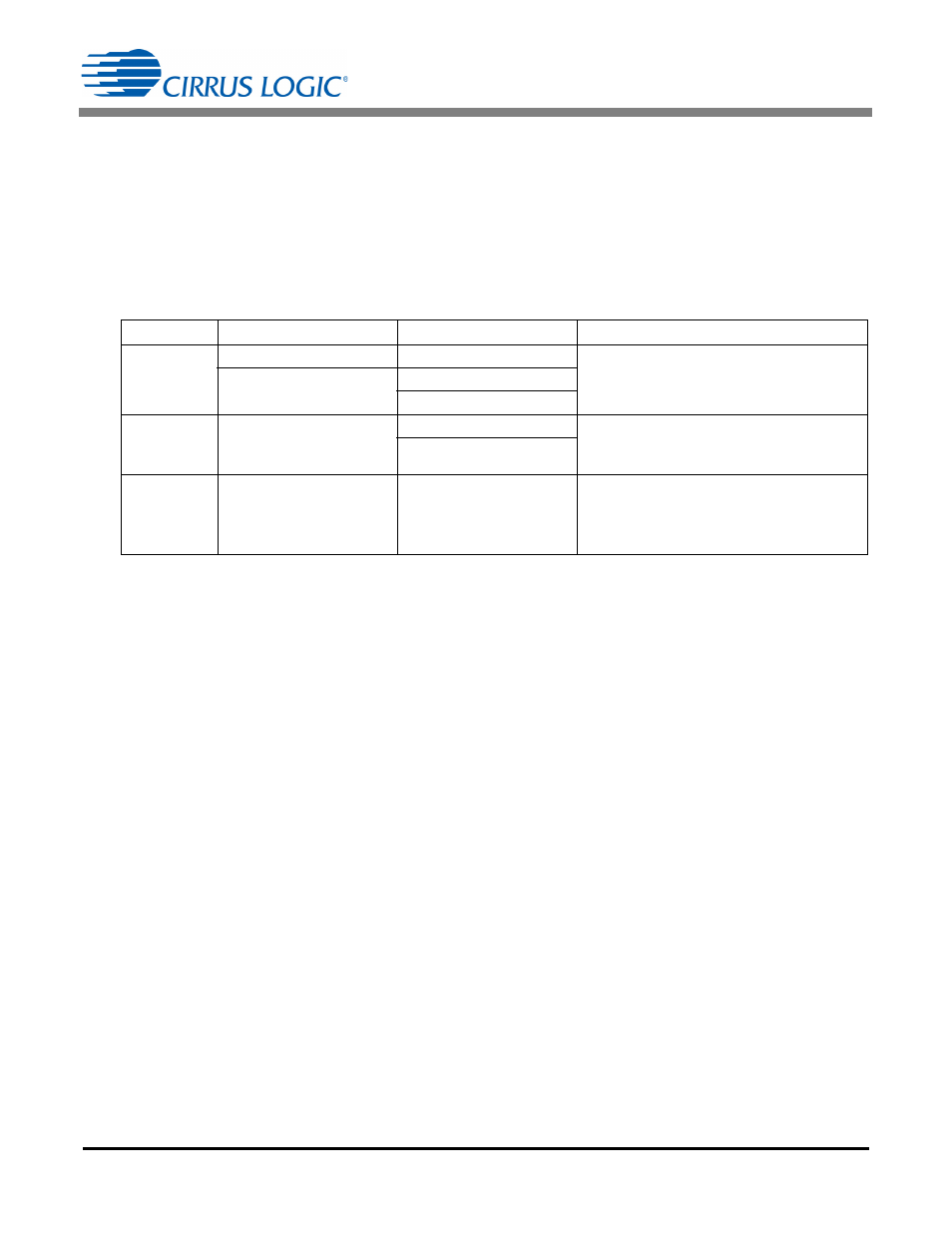
state of the IC (see Table 1 on page 14). The CS1680 dimmer switch detection algorithm is implemented using
a process of elimination: first, by a regular switch or a leading-edge dimmer paired with a magnetic
transformer; second, by a regular switch or a trailing-edge dimmer paired with an electronic transformer; third,
by a leading-edge dimmer paired with an electronic transformer.
The method of elimination is iterative and finds the best matching algorithm. The method of elimination
progresses through the detection algorithm to find the best matching state of operation. In an attempt to find
a dimmer compatible mode, the detection algorithm starts in Mode1, then tries Mode2, if Mode1 and Mode2
are excluded the algorithm defaults to Mode3.
The design process for the boost stage is outlined below:
1. Determine peak current I
BSTPK
and a tentative resistor value for resistor R
BST(Sense)
.
2. Select resistor R
CTRL1
used by the power algorithm.
3. Select resistor R
CTRL2
used by the electronic transformer algorithm.
4. Determine boost inductor specifications.
5. Calculate boost input and output capacitors.
6. Tune boost stage circuit power and electronic transformer algorithm by adjusting resistors R
CTRL1
and R
CTRL2
, respectively.
The boost stage utilizes a continuous current mode (CCM) control algorithm.
Step 11) Determine Boost Peak Current
Boost peak current I
BSTPK
is specific to each of the boost-stage algorithms. The required parameter
configuration for each boost-stage algorithm is given below:
1. The Mode1 algorithm has a peak current mode boost PFC based control. Maximum peak current
I
BSTPK(max)
is the only configurable parameter with regards to different boost inductors and output power
ratings.
2. The Mode3 algorithm is a constant power control where the reference current signal for the boost inductor
current is generated by dividing the input power required by the instantaneous rectified voltage signal. This
reference current is compared against the actual boost inductor current to control the duty cycle. Constant
power control ensures that the input current is at a minimum when the rectified input voltage is at the peak
and maximum when the rectified input voltage is at the trough. The Mode3 algorithm maximizes available
Boost Mode
Source
Line Switch
Digital Control Loop
Mode 1
12VAC/VDC
Non-dimming
Executes a boost peak-current algorithm
with PFC based control.
Magnetic Transformer
Leading-edge Dimmer
Non-dimming
Mode 2
Electronic Transformer
Trailing-edge Dimmer
Executes a constant boost peak-current
algorithm during the turn-on time of the
electronic transformer.
Non-dimming
Mode 3
Electronic Transformer
Leading-edge Dimmer
Executes a constant power control algo-
rithm where the boost inductor current is
controlled by the instantaneous rectified
voltage signal.
Table 1. Operating States