Step 8) buck inductor specification, Step 9) determine output capacitor, Step 10) zero-current detection – Cirrus Logic AN379 User Manual
Page 13: An379
AN379
AN379REV2
13
Step 8) Buck Inductor Specification
This step is the first iteration of the inductor design. Due to design constraints, the following requirements must
be met:
• The core must be big enough to fit the windings.
• The number of turns required must fit in the bobbin, along with insulation material.
• The finished inductor must not overheat in the environment.
• Magnetic and geometric constraints may not yield the exact value of inductor L
BUCK
.
Once the first iteration of the design is done, calculate the new period T1
BUCK
using the actual value of inductor
L
BUCK
, as shown in Equation 20:
Use Equation 21 to calculate the new switching period TT
BUCK(fb)
at full brightness using period T1
BUCK
:
Verify that the switch frequency at full brightness is within the desired range.
Step 9) Determine Output Capacitor
The buck output capacitor must provide a low impedance to the switching frequency. When using an
electrolytic capacitor, the choice is based on its ability to carry the ripple current to provide a long service life.
Meeting the ripple, voltage, temperature and lifetime requirements yields a high-value capacitor, often greater
than what is required for current handling. In buck applications, the voltage ripple across the output capacitor
is determined mostly by the ESR rather than the reactance.
Output capacitor C
OUT
RMS ripple current I
Ripple(RMS)
is the difference between the RMS current in the buck
inductor winding and the DC load current.
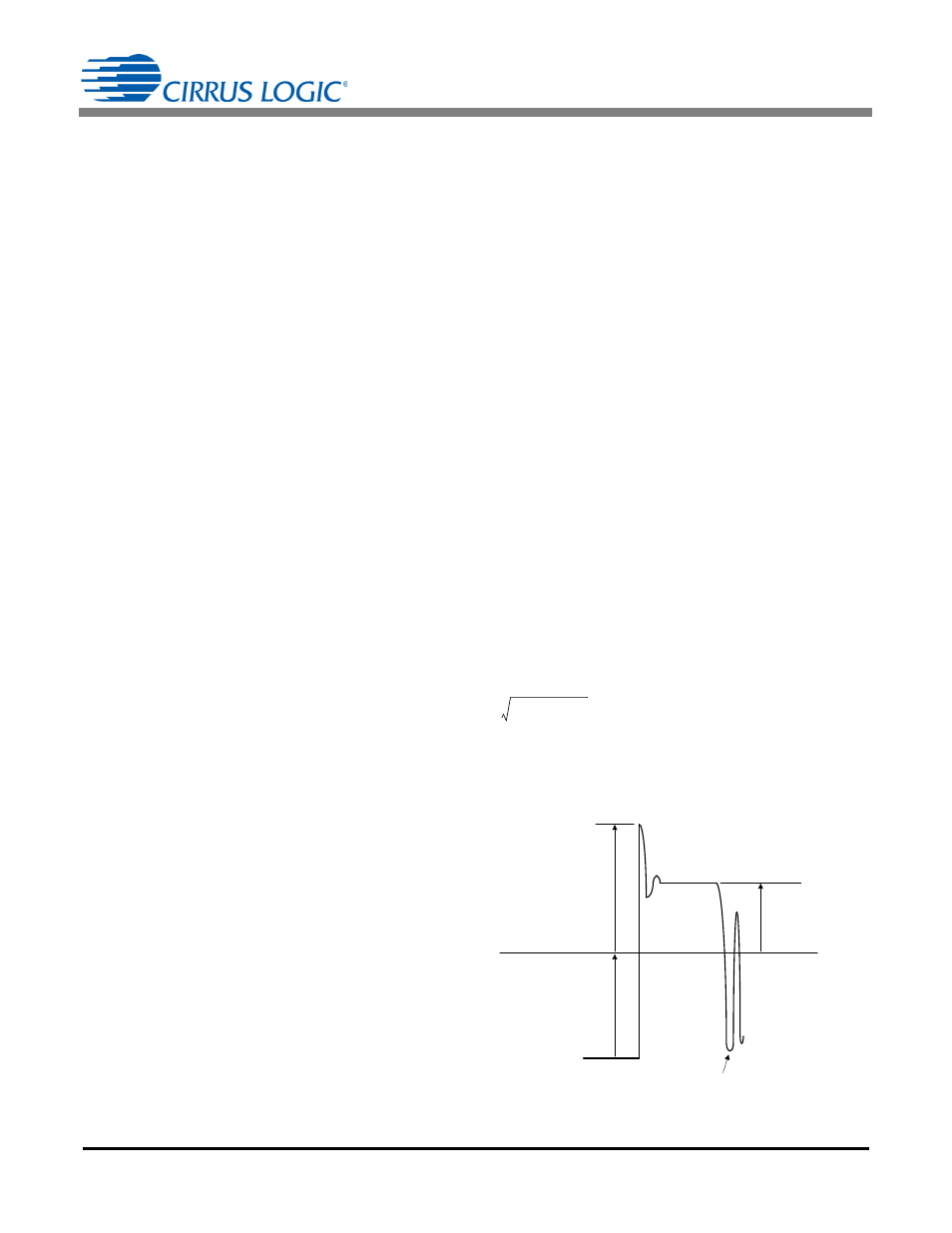
Step 10) Zero-current Detection
The CS1680 uses zero-current detection (ZCD) to minimize switching losses. The ZCD algorithm is designed
to turn on the buck power FET Q
BUCK
when the resonant voltage across the FET is at a low point
Figure 5 illustrates the zero-crossing switching
waveform. ZCD switching reduces the CV
2
power losses associated with the body
capacitance of the FET. The ZCD algorithm is
designed to monitor the resonant voltage at the
drain of the buck power FET.
The duration of period T1
BUCK
is determined by
the time it takes the inductor current to reach
peak current I
BUCKPK
, and the duration of
period T2
BUCK
is dependent on the time it takes
the demagnetization current to reach zero. Idle
time T3
BUCK
is initiated by the detection of the
first zero-crossing of the resonant voltage.
The zero-crossing switching waveform is
monitored by AC coupling the drain voltage of
FET Q
BUCK
to pin BUCKZCD. A series resistor
T1
BUCK max
I
BUCKPK
L
BUCK
V
BST max
V
OUT max
–
-------------------------------------------------------------------
=
[Eq. 20]
TT
BUCK fb
T1
BUCK
GAIN
TT
C min/max
-------------------------------------------------
=
[Eq. 21]
I
Ripple RMS
I
RMS
2
I
OUT
2
–
=
[Eq. 22]
First Valley
Buck FET
Drain Voltage
V
OUT
+ V
Diode
+V
P
V
BST
- V
OUT
V
OUT
+V
Diode
Figure 5. Switching Waveform of Buck FET Drain