General description, 1 pfc operation, Cs1601 – Cirrus Logic CS1601H User Manual
Page 9
CS1601
DS931F3
9
5. GENERAL DESCRIPTION
The CS1601 offers numerous features, options, and
functional capabilities to the electronic product lighting
designer. This digital power factor correction (PFC) control IC
is designed to replace legacy analog PFC controllers with
minimal design effort.
5.1 PFC Operation
One key feature of the CS1601 is its operating frequency
profile. Figure 10 illustrates how the frequency varies over a
half cycle of the line voltage in steady-state operation. When
power is first applied to the CS1601, it examines the line
voltage and adapts its operating frequency to the line voltage,
as shown in Figure 10. The operating frequency is varied from
the peak to the trough of the AC input. During startup, the
control algorithm generates maximum power while operating
in critical conduction mode (CRM), providing an approximate
square-wave current envelope within every half-line cycle.
Figure 10. Switching Frequency vs. Phase Angle
Figure 11 illustrates how the operating frequency of the
CS1601 (as a percentage of maximum frequency) changes
with output power and the peak of the line voltage.
Figure 11. CS1601 Max Switching Freq vs. Output Power
Figure 12 illustrates how the operating frequency of CS1601H
changes with output power and the peak of the line voltage.
Figure 12. CS1601H Max Switching Freq vs.Output Power
When P
O
falls below 5%, the CS1601 changes to Burst Mode.
on page 10 for more information.)
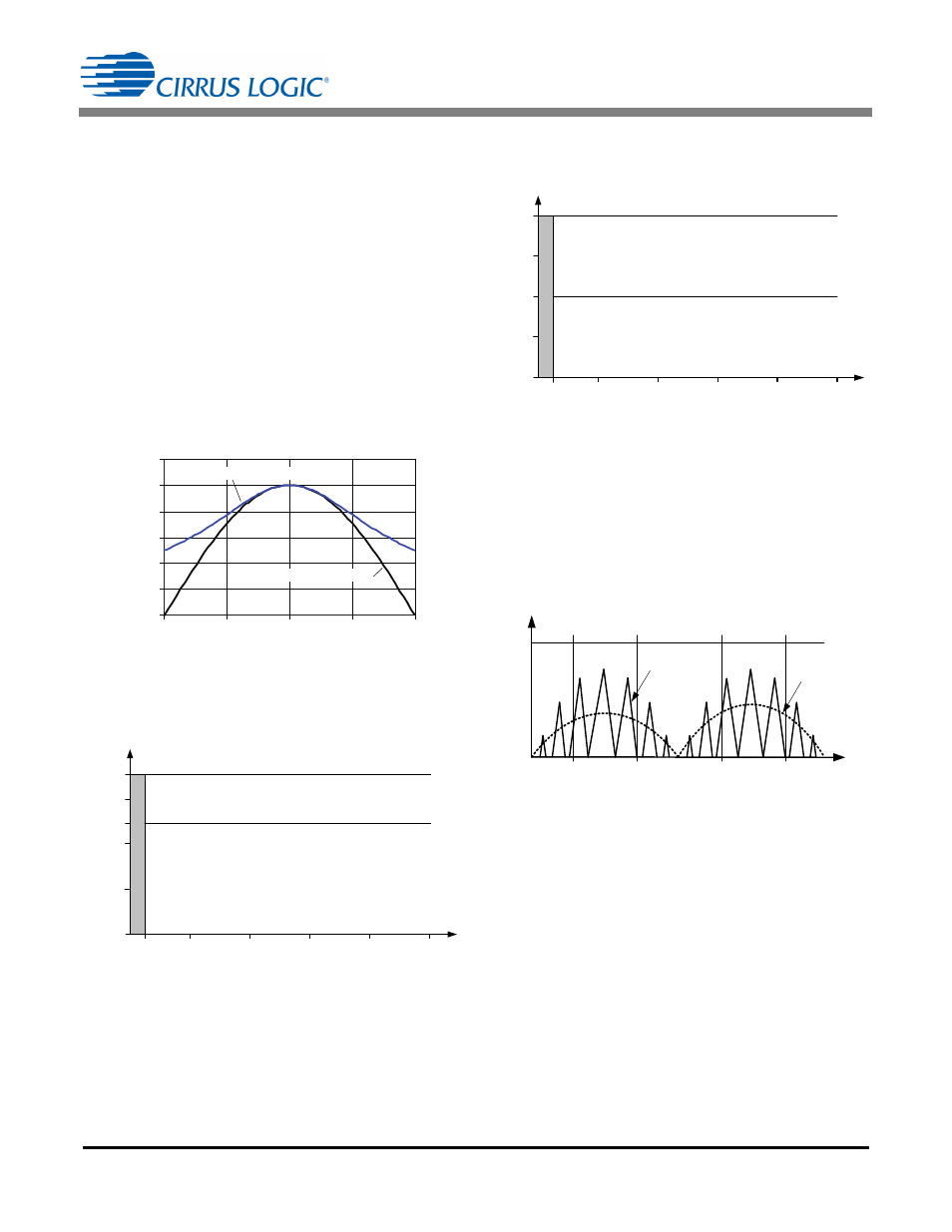
The CS1601 is designed to function as a DCM controller.
However, during peak periods, the controller may interchange
control methods and operate in a quasi-critical-conduction
mode (quasi-CRM) at low line. For example, at 108VAC main
input under full load, the PFC controller will function as a
quasi-CRM controller at the peak of the AC line cycle, as
shown in Figure 13.
Figure 13. DCM and Quasi-CRM Operation with CS1601
The zero-current detection (ZCD) of the boost inductor is
achieved using an auxiliary winding. When the stored energy
of the inductor is fully released to the output, the voltage on the
ZCD pin decreases, triggering a new switching cycle. This
quasi-resonant switching allows the active switch to be turned
on with near-zero inductor current, resulting in a nearly
lossless switch event. This minimizes turn-on losses and EMI
noise created by the switching cycle. PFC control is achieved
during light load by using on-time modulation.
0
20
40
60
80
100
120
0
45
90
135
180
Rectified Line Voltage Phase (Deg.)
% of Max
Switching Freq. (% of Max.)
Line Voltage (% of Max.)
% P
O max
F
SW
m
ax
(k
H
z)
20
70
60
40
40
5
Bu
rs
t M
od
e
20
0
60
80
100
48
Vin >156 VAC (Input Voltage 108 – 305 VAC, V
link
= 460V)
Vin <182 VAC (Input Voltage 108 –305 VAC , V
link
= 460V)
Vin <158 VAC (Input Voltage 90 –264 VAC, V
link
= 400 V)
Vin >136 VAC (Input Voltage 90 –264 VAC , V
link
= 400 V)
% P
O max
F
SW
m
a
x
(k
H
z)
100
75
Bu
rs
t M
od
e
25
0
50
Vin> 156 VAC (Input Voltage 108 –305 VAC , V
link
= 460V)
Vin< 182 VAC (Input Voltage 108 –305 VAC, V
link
= 460 V)
Vin< 158 VAC (Input Voltage 90– 264 VAC, V
link
= 400V)
Vin >136 VAC (Input Voltage 90 –264 VAC , V
link
= 400V)
20
40
5
60
80
100
DCM
Quasi CRM
DCM
Quasi CRM
DCM
I
LB
t [ms]
I
AC
In
du
ct
or
C
ur
re
n
t