2 startup vs. normal operation mode, 3 burst mode, 4 output power and pfc boost inductor – Cirrus Logic CS1601H User Manual
Page 10: Cs1601
CS1601
10
DS931F3
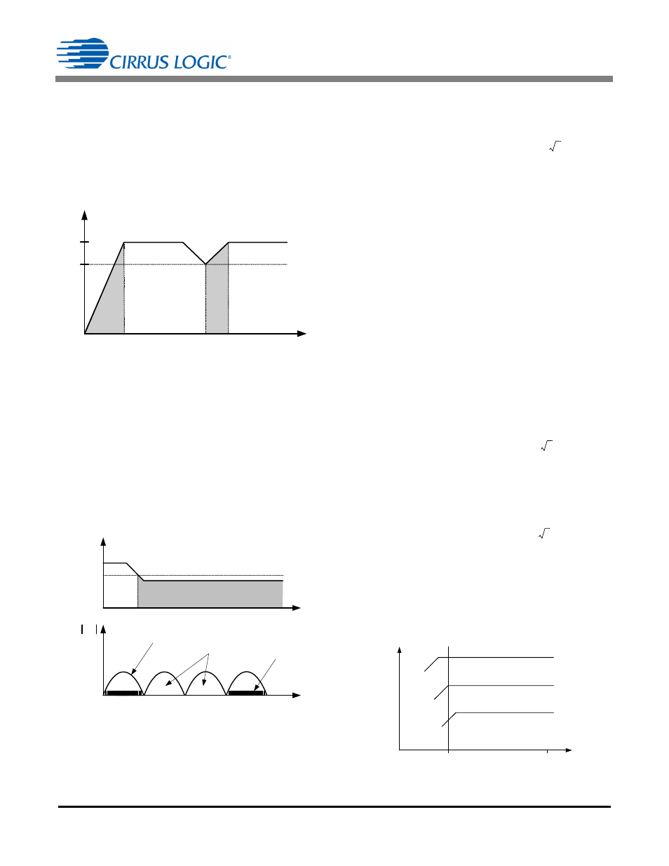
5.2 Startup vs. Normal Operation Mode
The CS1601 has two discrete operation modes: startup and
normal. Startup mode will be activated when V
link
is less than
90% of nominal value, V
O(startup)
, and remains active until V
link
reaches 100% of nominal value, as shown in Figure 14.
Startup mode is activated during initial system power-up. Any
V
link
drop to less than V
O(startup)
, such as a load change, can
cause the system to enter startup mode until V
link
is brought
back into regulation.
Figure 14. Startup and Normal Modes
Startup mode is defined as a surge of current delivering
maximum power to the output regardless of the load. During
every active switch cycle, the 'ON' time is calculated to drive a
constant peak current over the entire line cycle. However, the
'OFF' time is calculated based on the DCM/CCM boundary
equation.
5.3 Burst Mode
Burst mode is used to improve system efficiency when the
system output power (P
o
) is <5% of nominal. Burst mode is
implemented by intermittently disabling the PFC over a full
half-line period under light-load conditions, as shown in
Figure 15.
Figure 15. Burst Mode
5.4 Output Power and PFC Boost Inductor
In normal operating mode, the nominal output power is
estimated by the following equation:
where:
P
o
rated output power of the system
efficiency of the boost converter (estimated as 100%
by the PFC algorithm)
V
in(min)
minimum RMS line voltage measured after the
rectifier and EMI filter. V
in(min)
is equal to 90Vrms or
108 Vrms depending on the AC Line Voltage
operating range.
V
link
nominal PFC output voltage; V
link
= 400V when
V
i n ( m i n )
= 9 0 Vr m s o r V
l i n k
= 4 6 0 V w h e n
V
in(min)
= 108Vrms
f
max
maximum switching frequency; for the CS1601
f
max
= 70kHz and the CS1601H f
max
= 100kHz
L
B
boost inductor specified by rated power requirement
margin factor to guarantee rated output power (P
o
)
against boost inductor tolerances.
Equation 1 is provided for explanation purposes only. Using
substituted required design values for V
link
and f
max
gives the
following equation:
Changing the value for the V
link
voltage is not recommended.
Solving Equation 2 for the PFC boost inductor L
B
gives the
following equation:
If a value of the boost inductor other than that obtained from B , the link voltage V link will drop below 460V and fall out of regulation. Figure 16. Relative Effects of Varying Boost Inductance t [ms] V link [V] 100% 90% S tar tu p M od e Normal Mode S tar tu p M od e Normal Mode V in [V] t [ms] FET V gs Burst Mode Active V in P o [W] t [ms] PFC Disable Burst Threshold P o V in min 2 V link V in min 2 – 2 f max L B V link --------------------------------------------------------- = [Eq.1] P o 108V 2 460V 108V 2 – 2 70kHz L B 460V ------------------------------------------------------------- = [Eq.2] L B 108V 2 460V 108V 2 – 2 70kHz P o 460V ------------------------------------------------------------- = [Eq.3] V AC(rms) 108 305 P o (m ax) L > L B L = L B L < L B
Equation 3 above is used, the total output power capability
and the minimum input voltage threshold will differ according
to Equation 2. Note that if the input voltage drops below
108Vrms and the inductance value is