Introduction, Cs1601, Gnd ifb iac – Cirrus Logic CS1601H User Manual
Page 2: Stby

CS1601
2
DS931F3
1. INTRODUCTION
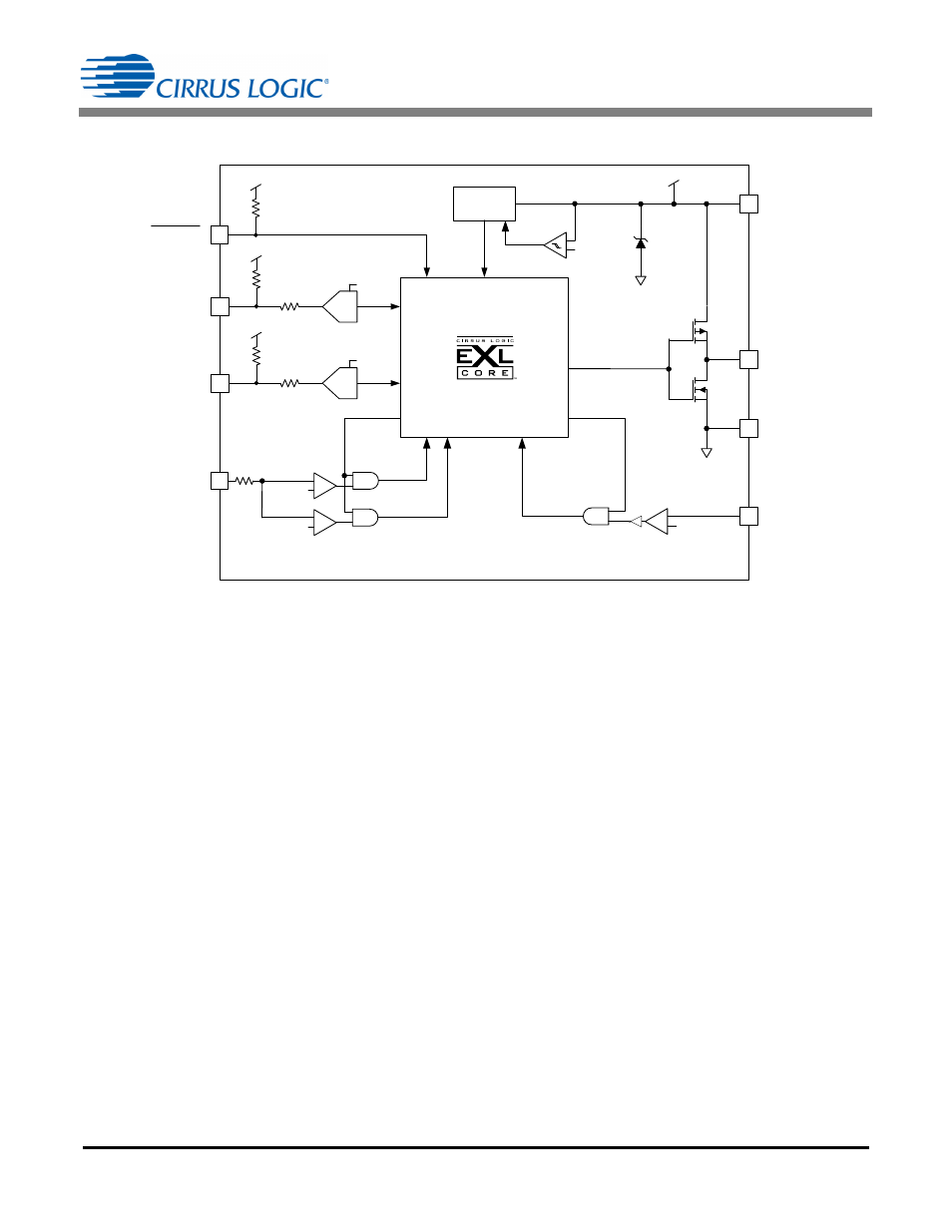
Figure 1. CS1601 Block Diagram
The CS1601 digital power factor correction (PFC) control IC is
designed to deliver the lowest system cost by reducing the
total number of system components and optimizing the EMI
noise signature, which reduces the conducted EMI filter
requirements. The CS1601 digital algorithm determines the
behavior of the
boost converter during startup, normal
operation, and under fault conditions (overvoltage,
overcurrent, and overtemperature).
Figure 1 illustrates a high-level block diagram of the CS1601.
The PFC processor logic regulates the power transfer by
using an adaptive digital algorithm to optimize the PFC active-
switch (MOSFET) drive signal duty cycle and switching
frequency. The adaptive controller uses independent analog-
to-digital converter (ADC) channels when sensing the
feedback and feedforward analog signals required to
implement the digital PFC control algorithm.
The AC mains rectified voltage (on pin IAC) and PFC output
link voltage (on pin IFB) are transformed by the PFC
processor logic and used to generate the optimum PFC
active-switch drive signal (GD) by calculating the optimal
switching frequency and t
ON
time on a cycle-by-cycle basis.
An auxiliary winding is typically added to the PFC boost
inductor to provide zero-current detection (ZCD) information.
The ZCD acts as a demagnetization sensor used to monitor
the PFC active-switching behavior and efficiency. The
auxiliary voltage is normalized using an external attenuator
and is connected to the ZCD pin, providing the CS1601 a
mechanism to detect the valley/zero crossings. The ZCD
comparator looks for the zero crossing on the auxiliary winding
and switches when the auxiliary voltage is below zero.
Switching in the valley of the oscillation minimizes the
switching losses and reduces EMI noise.
The PFC controller uses a current sensor for overcurrent
protection. The boost inductor peak current is measured
across an external resistor in the switching circuit on a cycle-
by-cycle basis. An overcurrent fault is generated when the
sense voltage applied to the CS pin exceeds a predefined
reference voltage.
The CS1601 includes a supervisor and protection circuit to
manage startup, shutdown, and fault conditions. The
protection circuit is designed to prevent output overvoltage as
a result of load and AC mains transients. The PFC power
converter main rectified voltage (V
rect
) and output link voltage
(V
link
) are monitored for overvoltage faults that would lead to
shutdown of the PFC controller. The PFC overvoltage
protection is designed for auto-recovery; operation resumes
once the fault clears.
V
Z
POR
+
-
V
DD( on)
V
DD( off)
Voltage
Regulator
8
VDD
5
ZCD
+
-
V
ZCD(th)
7
GD
Zero-Crossing
Detect
6
GND
IFB
IAC
V
DD
t
LEB
V
DD
15k
24k
3
V
DD
15k
24k
1
ADC
ADC
t
ZCB
4
CS
600
+
-
CS
Threshold
+
-
CS Clamp
V
CS (clamp)
V
CS (th)
STBY
V
DD
600k
2
I
ref
I
ref
