5 pfc output capacitor, 6 output ifb sense and input iac sense, 7 valley switching – Cirrus Logic CS1601H User Manual
Page 11: Cs1601, Zcd_below _zero
CS1601
DS931F3
11
5.5 PFC Output Capacitor
The value of the PFC output capacitor needs to be selected
based upon voltage ripple and hold-up requirements. To
ensure system stability with the digital controller, the
recommended value of the capacitor is within the range of
0.25
F/watt to 0.5F/watt with a V
link
voltage of 460V.
5.6 Output IFB Sense and Input IAC Sense
A current proportional to the PFC output voltage, V
link
, is
supplied to the IC on pin IFB and is used as a feedback control
signal. This current is compared against an internal fixed-
value reference current.
The ADC is used to measure the magnitude of the I
IFB
current
through resistor R
IFB
. The magnitude of the I
IFB
current is then
compared to an internal reference current of (I
ref
) 129
A.
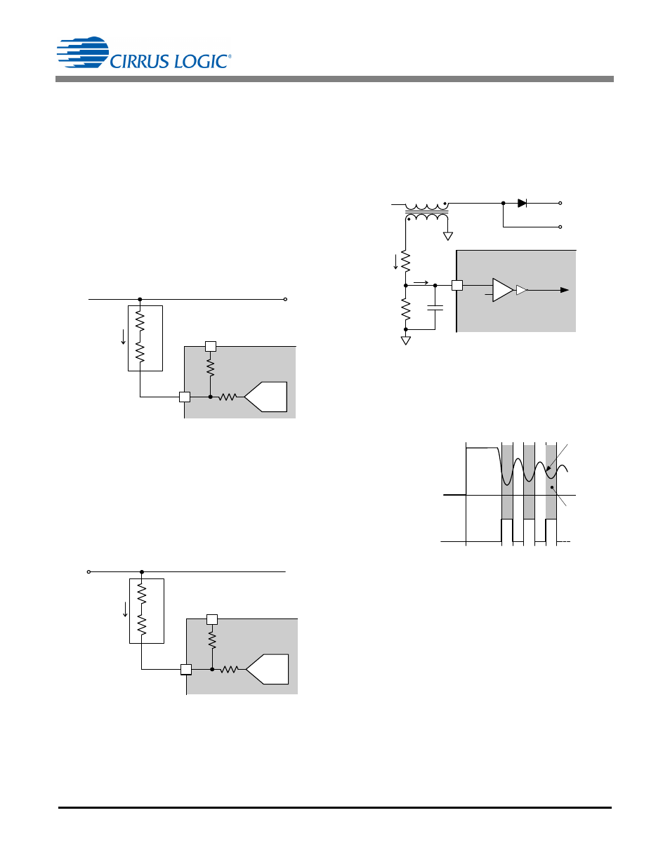
Figure 17. IFB Input Pin Model
Resistor R
IFB
sets the feedback current and is calculated as
follows:
By using digital loop compensation, the voltage feedback
signal does not require an external compensation network.
A current proportional to the AC input voltage is supplied to the
IC on pin IAC and is used by the PFC control algorithm.
Figure 18. IAC Input Pin Model
Resistor R
IAC
sets the IAC current and is derived as follows:
For optimal performance, resistors R
IAC
and
R
IFB
should use
1% tolerance or better resistors for best V
link
voltage accuracy.
5.7 Valley Switching
The zero-current detection (ZCD) pin is monitored for
demagnetization in the auxiliary winding of the boost inductor
(L
B
). The ZCD circuit is designed to detect the V
Aux
valley/zero crossings by sensing the voltage transformed onto
the auxiliary winding of L
B
.
Figure 19. ZCD Input Pin Model
The objective of zero-voltage switching is to initiate each
MOSFET switching cycle when its drain-source voltage is at
the lowest possible voltage potential, thus reducing switching
losses. The CS1601 uses an auxiliary winding on the PFC
boost inductor to implement zero-voltage switching.
Figure 20. Zero-voltage Switch
During each switching cycle, when the boost diode current
reaches zero, the boost MOSFET drain-source voltage begins
oscillating at the resonant frequency of the boost inductor and
MOSFET parasitic output capacitance. The ZCD_below_zero
signal transitions from high to low just prior to a local minimum
of the MOSFET drain-source voltage oscillation. The zero-
crossing detect circuit ensures that a ZCD_below_zero pulse
will only be generated when the comparator output is
continuously high for a nominal time period (t
ZCB
) of 200ns.
Therefore, any negative edges on the comparator's output
due to spurious glitches will not cause a pulse to be
generated.
Due to the CS1601's variable-frequency control, the MOSFET
switching cycle will not always be initiated at the first resonant
valley. The external circuitry should be designed so that the
current (I
ZCD
) at the ZCD pin is approximately ±1.0mA. The
IFB
V D D
15 k
8
V
link
CS1601
24k
ADC
R5
R
IFB
I
FB
R6
1
R
IFB
V
link
V
DD
–
I
ref
-----------------------------
460V V
DD
–
129
A
-------------------------------
=
=
[Eq.4]
R1
R
IAC
I
AC
IA C
V D D
15 k
8
V
rec t
CS1601
24 k
ADC
R2
3
R
IAC
R
IFB
=
[Eq.5]
R3
I
Aux
V
link
ZCD
L
B
R4
CS1601
ZCD_below_zero
D2
FE T Drain
N:1
+
V
Aux
-
Demag
Comparator
+
-
V
th( Z CD)
5
I
Z CD
C
p
ZCD
Zero Crossing
Detection
GD ‘ON’
ZCD_below _zero