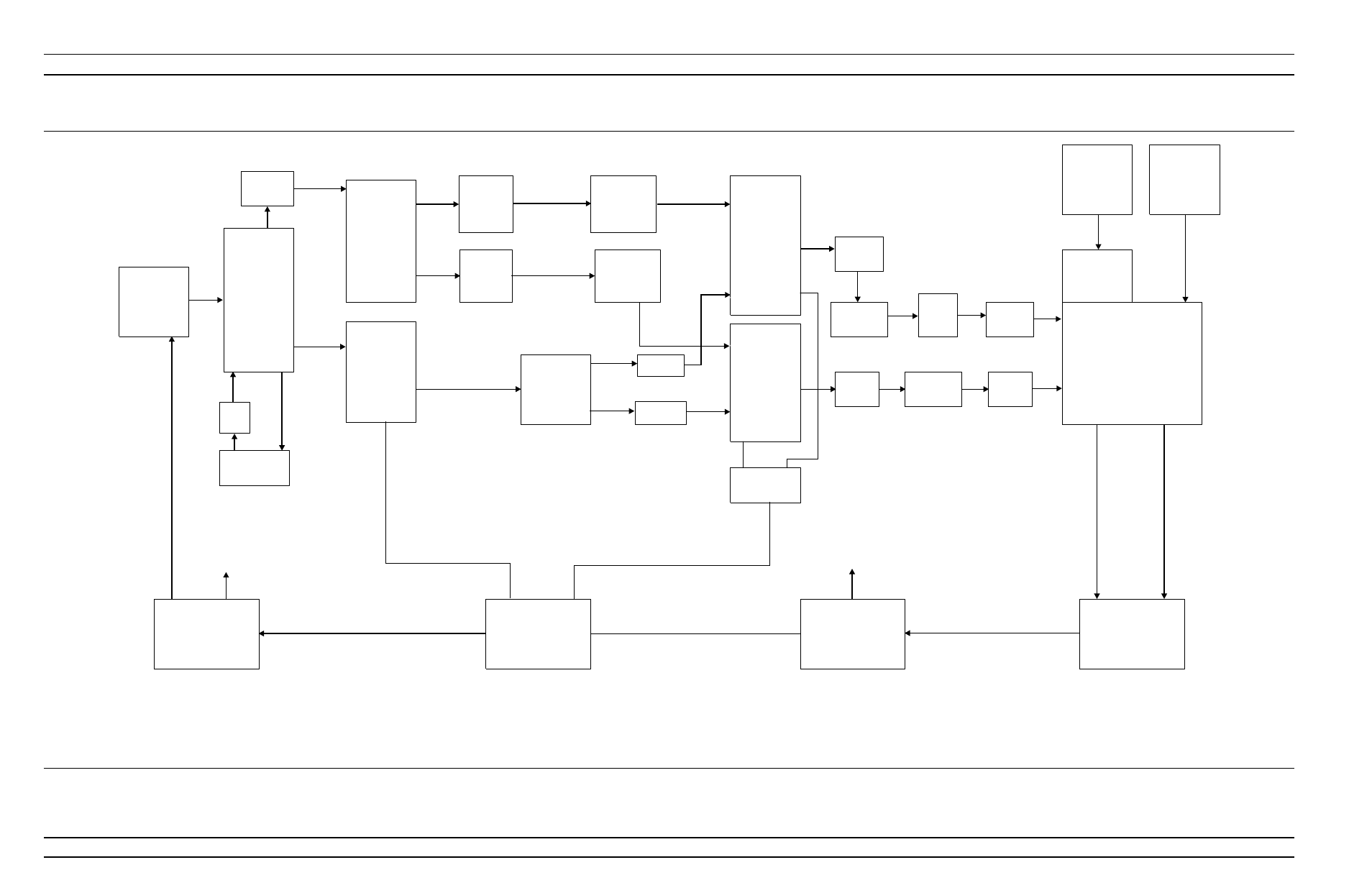
Signal paths troubleshooting, Figure 5-4 – Anritsu 373XXA User Manual
Page 80
5-26
373XXA MM
SIGNAL PATHS
TROUBLESHOOTING
YIG Oscillator
X4
(SQM)
Reverse
Switched Filter
Down
Converter
A21A2 PCB
Sampler/Buffer Amp
X2
(SDM)
3 dB pad
X4
(SQM)
Forward
MUX Coupler
(reverse)
3 dB Pad
Transfer Switch
(Ref A/ Ref B
Control)
37 GHz
HiPass Filter
37 GHz
HiPass Filter
Shaped Pad
Shaped Pad
MUX Coupler
(forward)
A21A1 PCB
A4 PCB
Reference IF Processor
SPDT Switch
J4
J5
Ref A
Ref B 38-65 GHz
Ref A 38-65 GHz
Ref B
A8 PCB
Source Lock/ RF
Component Control
Power Amp
Second LO
(A2 PCB)
(25-272MHz)
First LO
(A1 PCB)
(357-536MHz)
Ref A 40MHz - 38GHz
Ref B 40MHz - 38GHz
Rear
Panel
Access
Loop **
40MHz-65GHz (Ref A)
40MHz -
65GHz (Ref B)
ALC Control PCB
49808-3
Ref A
J7
J8
Ref B
2.5 MHz CW
2.5 MHz CW
J4
J2
J1
J1
J3
Ref A 38-65 GHz
Ref B
DC
voltage
38-65
GHz
DC voltage (6 MHz / Volt)
J4
J1
J4
J4
J5
J5
DCV
DCV
J1
J3
J2
YIG tuning currents
Digital and Analog Control
40MHz-
2GHz
6.3-
8.3GHz
2-20GHz
40MHz-
19GHz
9.5-
16.25GHz
40MHz-38GHz
SDM Control
Bias Voltages to YIG,
Switched Filter
Down Converter, SAM
Control of SPDT
switch, transfer switch,
buffer amp, power
amp, ALC control
J5
J5
J3
J1
3 dB pad
3 dB pad
16.8 GHz
Lowpass
Filter
15 dB
Pad
NOTE: Sampler/Buffer amplifiers are individually matched to
Power Amplifiers. If either fails, both should be replaced with
another matched set, part number ND53249.
3 dB Pad
** Indicates not present on model 37297B or 37277B
3 dB pad
Figure 5-4.
37397A Source Lock Signal Path Diagram