Pcb layout recommendations, Ad9883a – Analog Devices AD9883A User Manual
Page 22
REV. 0
AD9883A
–22–
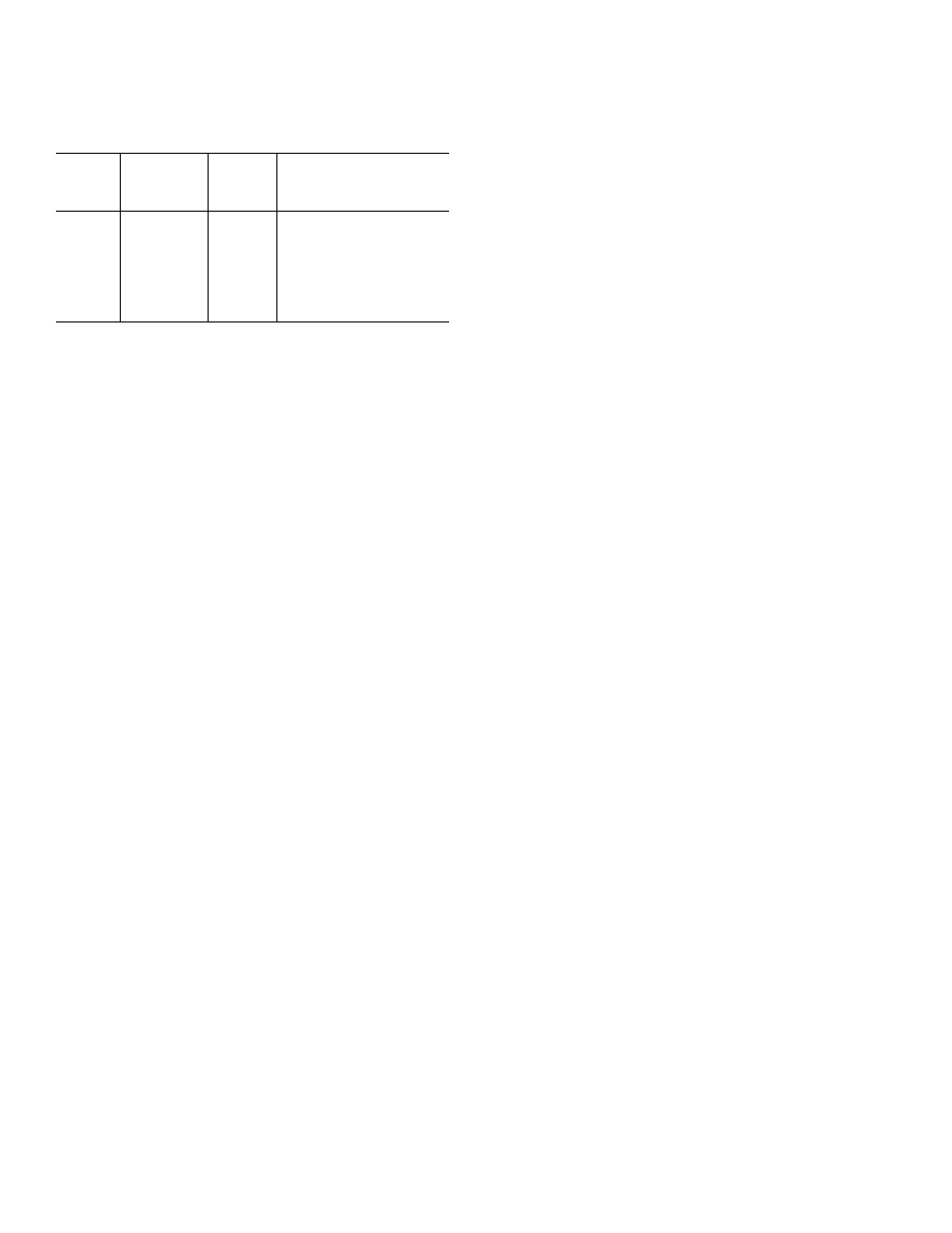
Table XXXVIII. Control of the Sync Block Muxes via the
Serial Register
Control
Mux
Serial Bus
Bit
Nos.
Control Bit
State
Result
1 and 2
0EH: Bit 3
0
Pass Hsync
1
Pass Sync-on-Green
3
0FH: Bit 5
0
Pass Coast
1
Pass Vsync
4
0EH: Bit 0
0
Pass Vsync
1
Pass Sync Separator Signal
Sync Slicer
The purpose of the sync slicer is to extract the sync signal from
the green graphics channel. A sync signal is not present on all
graphics systems, only those with “sync-on-green”. The sync
signal is extracted from the green channel in a two-step process.
First, the SOG input is clamped to its negative peak, (typically
0.3 V below the black level). Next, the signal goes to a com-
parator with a variable trigger level, nominally 0.15 V above the
clamped level. The “sliced” sync is typically a composite sync
signal containing both Hsync and Vsync.
Sync Separator
A sync separator extracts the Vsync signal from a composite
sync signal. It does this through a low-pass filter-like or integrator-
like operation. It works on the idea that the Vsync signal stays
active for a much longer time than the Hsync signal, so it
rejects any signal shorter than a threshold value, which is some-
where between an Hsync pulsewidth and a Vsync pulsewidth.
The sync separator on the AD9883A is simply an 8-bit digital
counter with a 5 MHz clock. It works independently of the
polarity of the composite sync signal. (Polarities are determined
elsewhere on the chip.) The basic idea is that the counter counts
up when Hsync pulses are present. But since Hsync pulses are
relatively short in width, the counter only reaches a value of N
before the pulse ends. It then starts counting down eventually
reaching 0 before the next Hsync pulse arrives. The specific
value of N will vary for different video modes, but will always be
less than 255. For example with a 1
µs width Hsync, the counter
will only reach 5 (1
µs/200 ns = 5). Now, when Vsync is present
on the composite sync the counter will also count up. However,
since the Vsync signal is much longer, it will count to a higher
number M. For most video modes, M will be at least 255. So,
Vsync can be detected on the composite sync signal by detecting
when the counter counts to higher than N. The specific count
that triggers detection (T) can be programmed through the
serial register (0fh).
Once Vsync has been detected, there is a similar process to detect
when it goes inactive. At detection, the counter first resets to 0,
then starts counting up when Vsync goes away. Similar to the
previous case, it will detect the absence of Vsync when the
counter reaches the threshold count (T). In this way, it will
reject noise and/or serration pulses. Once Vsync is detected to
be absent, the counter resets to 0 and begins the cycle again.
PCB LAYOUT RECOMMENDATIONS
The AD9883A is a high precision, high speed analog device. As
such, to get the maximum performance out of the part it is
important to have a well laid-out board. The following is a guide
for designing a board using the AD9883A.
Analog Interface Inputs
Using the following layout techniques on the graphics inputs is
extremely important.
Minimize the trace length running into the graphics inputs. This
is accomplished by placing the AD9883A as close as possible
to the graphics VGA connector. Long input trace lengths are
undesirable because they will pick up more noise from the board
and other external sources.
Place the 75
Ω termination resistors (see Figure 1) as close to the
AD9883A chip as possible. Any additional trace length between
the termination resistors and the input of the AD9883A increases
the magnitude of reflections, which will corrupt the graphics signal.
Use 75
Ω matched impedance traces. Trace impedances other
than 75
Ω will also increase the chance of reflections.
The AD9883A has very high input bandwidth, (500 MHz). While
this is desirable for acquiring a high-resolution PC graphics
signal with fast edges, it means that it will also capture any high-
frequency noise present. Therefore, it is important to reduce the
amount of noise that gets coupled to the inputs. Avoid running
any digital traces near the analog inputs.
Due to the high bandwidth of the AD9883A, sometimes low-
pass filtering the analog inputs can help to reduce noise. (For
many applications, filtering is unnecessary.) Experiments have
shown that placing a series ferrite bead prior to the 75
Ω termi-
nation resistor is helpful in filtering out excess noise.
Specifically, the part used was the # 2508051217Z0 from Fair-
Rite, but each application may work best with a different bead
value. Alternately, placing a 100
Ω to 120 Ω ohm resistor between
the 75
Ω termination resistor and the input coupling capacitor
can also benefit.
Power Supply Bypassing
It is recommended to bypass each power supply pin with a
0.1
µF capacitor. The exception is in the case where two or
more supply pins are adjacent to each other. For these group-
ings of powers/grounds, it is only necessary to have one bypass
capacitor. The fundamental idea is to have a bypass capacitor
within about 0.5 cm of each power pin. Also, avoid placing the
capacitor on the opposite side of the PC board from the AD9883A,
as that interposes resistive vias in the path.
The bypass capacitors should be physically located between the
power plane and the power pin. Current should flow from the
power plane to the capacitor to the power pin. Do not make the
power connection between the capacitor and the power pin.
Placing a via underneath the capacitor pads, down to the power
plane, is generally the best approach.
It is particularly important to maintain low noise and good
stability of PV
D
(the clock generator supply). Abrupt changes in
PV
D
can result in similarly abrupt changes in sampling clock
phase and frequency. This can be avoided by careful attention
to regulation, filtering, and bypassing. It is highly desirable to
provide separate regulated supplies for each of the analog cir-
cuitry groups (V
D
and PV
D
).
Some graphic controllers use substantially different levels of
power when active (during active picture time) and when idle
(during horizontal and vertical sync periods). This can result in
a measurable change in the voltage supplied to the analog supply
regulator, which can in turn produce changes in the regulated
analog supply voltage. This can be mitigated by regulating the
analog supply, or at least PV
D
, from a different, cleaner power
source (for example, from a 12 V supply).