Wire serial control port, Serial port read/write timing, Ad9883a – Analog Devices AD9883A User Manual
Page 20
REV. 0
AD9883A
–20–
Table XXXIV. Detected Coast Input Polarity Status
Hsync Polarity Status
Result
0
Coast Polarity Negative
1
Coast Polarity Positive
15
7
4:2:2 Output Mode Select
A bit that configures the output data in 4:2:2 mode.
This mode can be used to reduce the number of data
lines used from 24 down to 16 for applications using
YUV, VCbCr, or PbPr graphics signals. A timing dia-
gram for this mode is shown in Figure 9.
Recommended input and output configurations are
shown in Table XXXV. In 4:2:2 mode, the red and
blue channels can be interchanged to help satisfy board
layout or timing requirements, but the green channel
must be configured for Y.
Table XXXV. 4:2:2 Output Mode Select
Select
Output Mode
0
4:4:4
1
4:2:2
Table XXXVI. 4:2:2 Input/Output Configuration
Input
Channel
Connection
Output Format
Red
V
U/V
Green
Y
Y
Blue
U
High Impedance
2-WIRE SERIAL CONTROL PORT
A 2-wire serial interface control interface is provided. Up to four
AD9883A devices may be connected to the 2-wire serial inter-
face, with each device having a unique address.
The 2-wire serial interface comprises a clock (SCL) and a bidi-
rectional data (SDA) pin. The Analog Flat Panel Interface acts
as a slave for receiving and transmitting data over the serial inter-
face. When the serial interface is not active, the logic levels on
SCL and SDA are pulled high by external pull-up resistors.
Data received or transmitted on the SDA line must be stable for
the duration of the positive-going SCL pulse. Data on SDA must
change only when SCL is low. If SDA changes state while SCL
is high, the serial interface interprets that action as a start or
stop sequence.
There are five components to serial bus operation:
• Start Signal
• Slave Address Byte
• Base Register Address Byte
• Data Byte to Read or Write
• Stop Signal
When the serial interface is inactive (SCL and SDA are high)
communications are initiated by sending a start signal. The start
signal is a high-to-low transition on SDA while SCL is high.
This signal alerts all slaved devices that a data transfer sequence
is coming.
The first eight bits of data transferred after a start signal com-
prising a 7-bit slave address (the first seven bits) and a single R/
W
bit (the eighth bit). The R/
W bit indicates the direction of data
transfer, read from (1) or write to (0) the slave device. If the
transmitted slave address matches the address of the device (set by
the state of the SA
1-0
input pins in Table XXXIV, the AD9883A
acknowledges by bringing SDA LOW on the 9th SCL pulse. If
the addresses do not match, the AD9883A does not acknowledge.
Table XXXVII. Serial Port Addresses
Bit 7
Bit 6
Bit 5
Bit 4
Bit 3
Bit 2
Bit 1
A
6
A
5
A
4
A
3
A
2
A
1
A
0
(MSB)
1
0
0
1
1
0
0
1
0
0
1
1
0
1
Data Transfer via Serial Interface
For each byte of data read or written, the MSB is the first bit of
the sequence.
If the AD9883A does not acknowledge the master device during
a write sequence, the SDA remains high so the master can
generate a stop signal. If the master device does not acknowledge
the AD9883A during a read sequence, the AD9883A interprets
this as “end of data.” The SDA remains high so the master
can generate a stop signal.
Writing data to specific control registers of the AD9883A requires
that the 8-bit address of the control register of interest be written
after the slave address has been established. This control register
address is the base address for subsequent write operations. The
base address autoincrements by one for each byte of data written
after the data byte intended for the base address. If more bytes
are transferred than there are available addresses, the address will
not increment and remains at its maximum value of 14h. Any base
address higher than 14h will not produce an acknowledge signal.
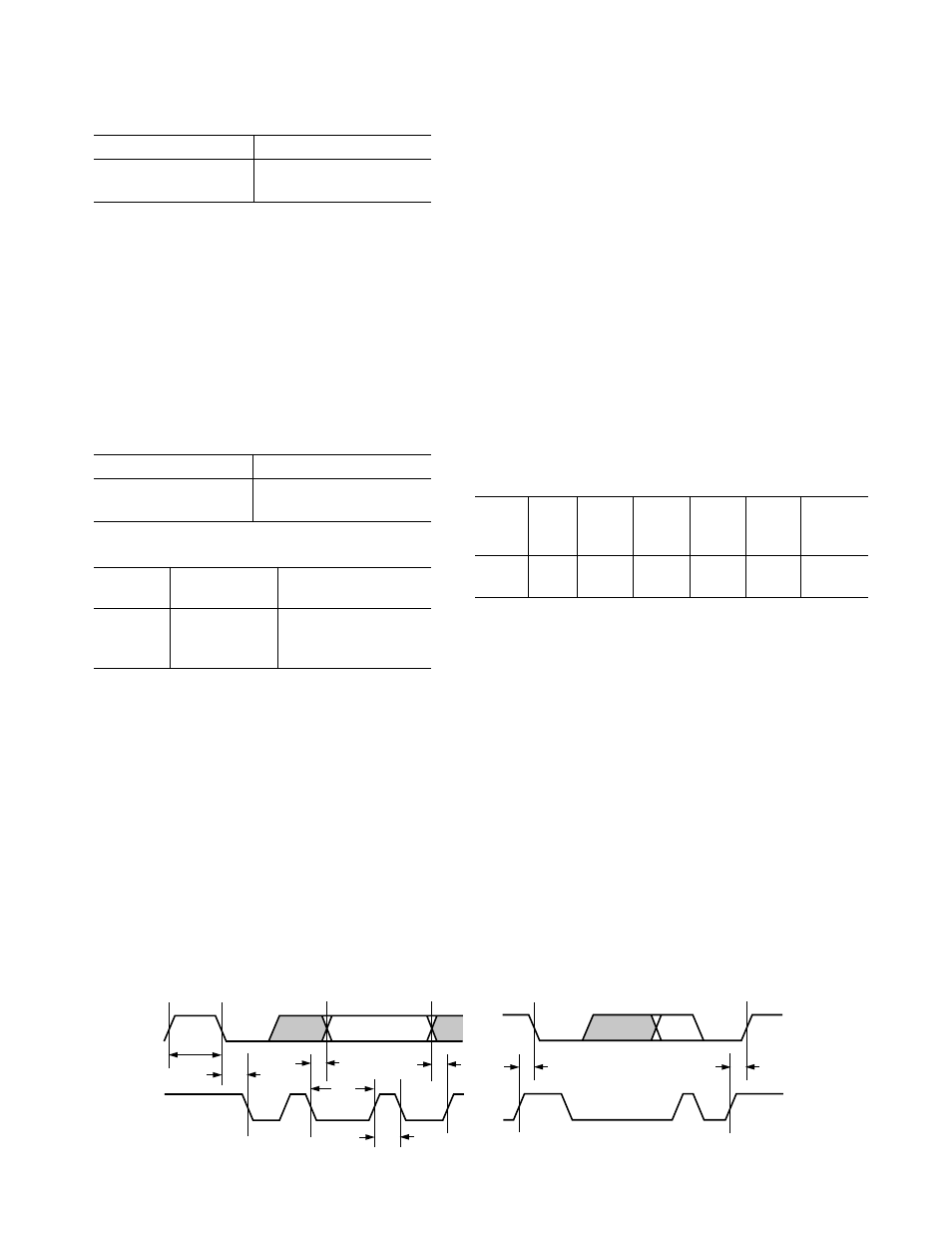
SDA
SCL
t
BUFF
t
STAH
t
DHO
t
DSU
t
DAL
t
DAH
t
STASU
t
STOSU
Figure 10. Serial Port Read/Write Timing