Ad9883a – Analog Devices AD9883A User Manual
Page 13
REV. 0
AD9883A
–13–
2-Wire Serial Register Map
The AD9883A is initialized and controlled by a set of registers, which determine the operating modes. An external controller is
employed to write and read the Control Registers through the 2-line serial interface port.
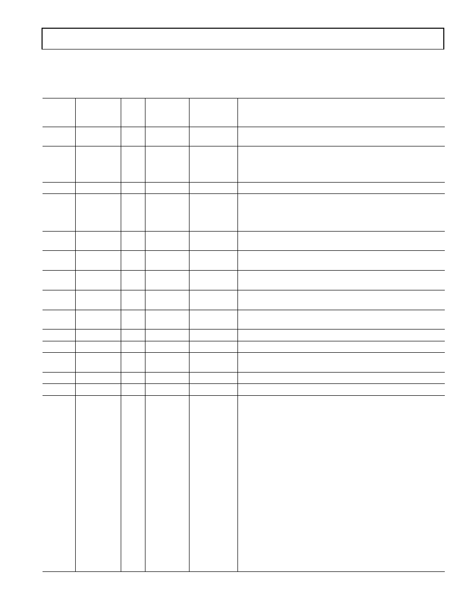
Table VI. Control Register Map
Write and
Hex
Read or
Default
Register
Address
Read Only
Bits
Value
Name
Function
00H
RO
7:0
Chip Revision
An 8-bit register that represents the silicon revision level.
Revision 0 = 0000 0000
01H
R/
W
7:0
01101001
PLL Div MSB
This register is for Bits [11:4] of the PLL divider. Larger values mean
the PLL operates at a faster rate. This register should be loaded first
whenever a change is needed. (This will give the PLL more time to
lock.) See Note 1 .
02H
R/
W
7:4
1101
****
PLL Div LSB
Bits [7:4] LSBs of the PLL divider word. See Note 1.
03H
R/
W
7:3
01
******
Bits [7:6] VCO Range. Selects VCO frequency range. (See PLL
description.)
**001***
Bits [5:3] Charge Pump Current. Varies the current that drives the
low-pass filter. (See PLL description.)
04H
R/
W
7:3
01000
***
Phase Adjust
ADC Clock Phase Adjustment. Larger values mean more delay.
(1 LSB = T/32.)
05H
R/
W
7:0
10000000
Clamp
Places the Clamp signal an integer number of clock periods after the trail-
Placement
ing edge of the HSYNC signal.
06H
R/
W
7:0
10000000
Clamp
Number of clock periods that the Clamp signal is actively clamping.
Duration
07H
R/
W
7:0
00100000
Hsync Output
Sets the number of pixel clocks that HSOUT will remain active.
Pulsewidth
08H
R/
W
7:0
10000000
Red Gain
Controls ADC input range (Contrast) of each respective channel.
Bigger values give less contrast.
09H
R/
W
7:0
10000000
Green Gain
0AH
R/
W
7:0
10000000
Blue Gain
0BH
R/
W
7:1
1000000
*
Red Offset
Controls dc offset (Brightness) of each respective channel. Bigger
values decrease brightness.
0CH
R/
W
7:1
1000000
*
Green Offset
0DH
R/
W
7:1
1000000
*
Blue Offset
0EH
R/
W
7:0
0
*******
Sync Control
Bit 7 – Hsync Polarity Override. (Logic 0 = Polarity determined by
chip, Logic 1 = Polarity set by Bit 6 in register 0Eh.)
*1******
Bit 6 – Hsync Input Polarity. Indicates polarity of incoming HSYNC
signal to the PLL. (Logic 0 = Active Low, Logic 1 = Active High.)
**0*****
Bit 5 – Hsync Output Polarity. (Logic 0 = Logic High Sync, Logic 1 =
Logic Low Sync.)
***0****
Bit 4 – Active Hsync Override. If set to Logic 1, the user can select
the Hsync to be used via Bit 3. If set to Logic 0, the active interface
is selected via Bit 6 in register 14H.
****0***
Bit 3 – Active Hsync Select. Logic 0 selects Hsync as the active
sync. Logic 1 selects Sync-on-Green as the active sync. Note: The
indicated Hsync will be used only if Bit 4 is set to Logic 1 or if both
syncs are active, (Bits 1, 7 = Logic 1 in register 14H).
*****0**
Bit 2 – Vsync Output Invert. (Logic 0 = No Invert, Logic 1 = Invert.)
******0*
Bit 1 – Active Vsync Override. If set to Logic 1, the user can select
the Vsync to be used via Bit 0. If set to Logic 0, the active interface
is selected via Bit 3 in register 14H.
*******0
Bit 0 – Active Vsync Select. Logic 0 selects Raw Vsync as the output
Vsync. Logic 1 selects Sync Separated Vsync as the output Vsync.
Note: The indicated
Vsync will be used only if Bit 1 is set to Logic 1.