Communication Concepts FM-1KW Broadcast Application Note User Manual
Page 6
6
RF Reference Design Data
Freescale Semiconductor
MRFE6VP61K25H MRFE6VP61K25HS FM Broadcast
FREESCALE RF POWER 50 V TECHNICAL ADVANTAGES
50 V Drain Voltage
The 87.5--108 MHz FM broadcast reference design fixture
was designed to utilize the standard 50 volt power supply
commonly used in this market.
Data was collected to characterize the reference design’s
output power and efficiency vs. drain voltage, as shown in
Figure 8. The output power can be adjusted over a 12 dB
worth of dynamic range by adjusting the drain voltage, while
creating minimal degradation on the efficiency performance.
Refer to Freescale’s 50 V RF LDMOS White Paper. Go to
http://freescale.com/RFpower and select Documentation/-
White Papers -- 50VRFLDMOSWP for more information
on 50 V RF LDMOS technology.
1200
10
1000
800
90
80
75
70
V
DD
, DRAIN VOLTAGE (VOLTS)
Figure 8. Output Power and Drain Efficiency
versus Drain Voltage
P
out
,O
UT
PU
T
POWER
(W
ATTS)
η
D,
DRA
IN
EF
FI
CIE
NCY
(%
)
η
D
0
55
P
out
400
P
in
= 3.5 W
f = 98 MHz
I
DQ
= 200 mA
600
200
85
65
60
20
30
40
50
5
15
25
35
45
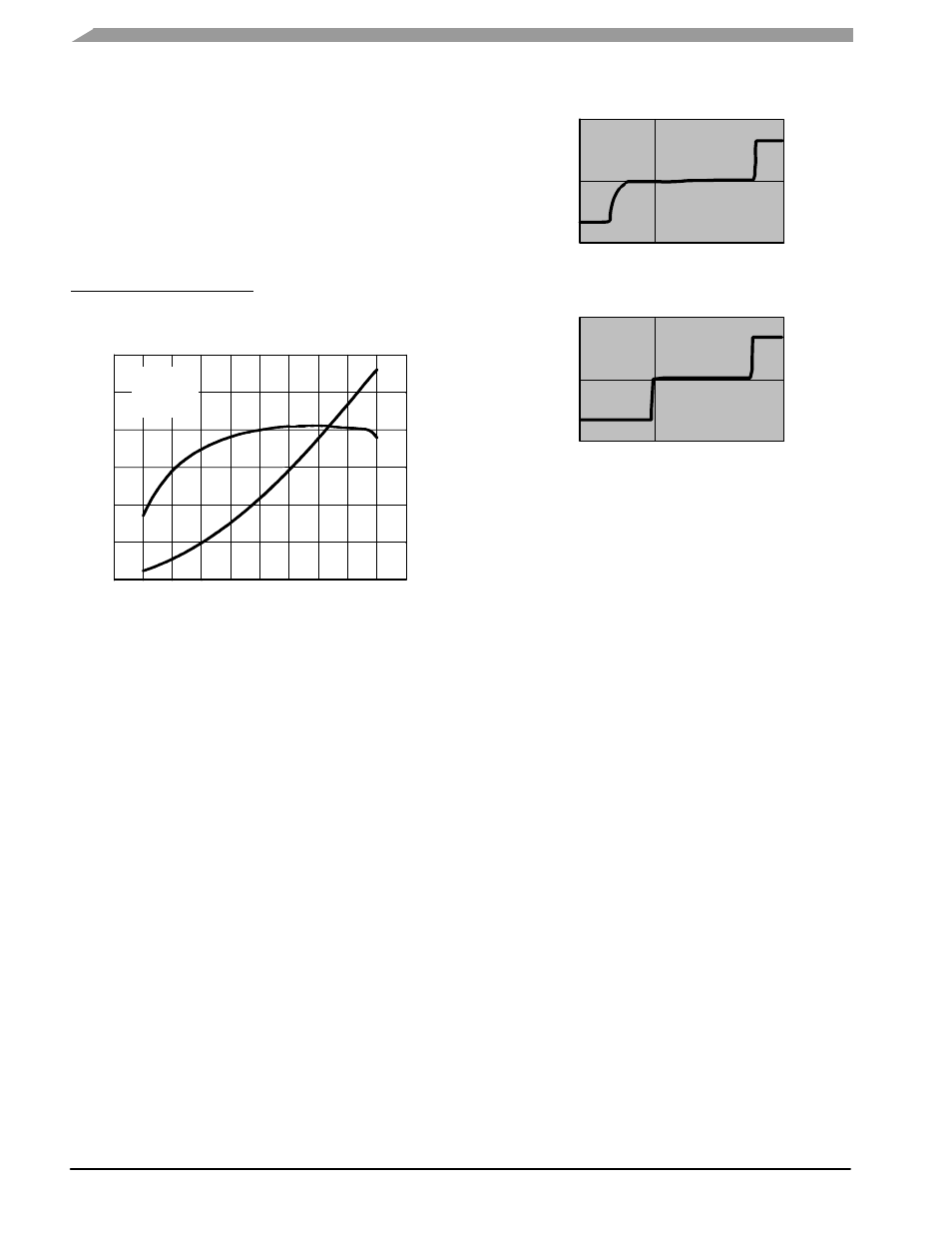
Extended Gate Voltage Range
The enhanced electrostatic discharge (ESD) protection
structure at the gate of the transistor is a Freescale
innovation pioneered in the cellular infrastructure market that
is incorporated into the 50 volts RF LDMOS power product
portfolios. This ESD structure can tolerate moderate reverse
bias conditions, applied to the gate lead, up to --6 volts as
shown in Figure 9. This allows these transistors to be used in
zero gate voltage, Class C bias applications where the RF
voltage swings on the gate can be significantly lower than the
ground potential.
Figure 9. Gate Voltage Breakdown with ESD
2.E--02
0.E+00
--2.E--02
--1.E--02
--5.E--03
5.E--03
1.E--02
--15
0
--10 --5
5 10 15
20
25
V
GS
(V)
I
ESD
(A
)
Enhanced ESD
2.E--02
0.E+00
--2.E--02
--1.E--02
--5.E--03
5.E--03
1.E--02
--15
0
--10 --5
5 10 15
20
25
V
GS
(V)
I
ESD
(A
)
Standard ESD
High Ruggedness/Energy Absorption
The MRFE6VP61K25H/HS was designed to operate in
applications which demand very high ruggedness. The
VHV6E technology has proven to be valuable in FM broad-
cast applications, specifically in high definition (HD) FM
transmitters where a high peak--to--average (PAR) digital sig-
nal is injected on top of an existing analog FM signal. At the
peak of the signal, the voltage waveform could exceed the
V
(BR)DSS
breakdown voltage of the device and thus cause
the device to enter into an avalanche condition. However, for
the device to fail, the current must be sufficiently high enough
during the high voltage period to activate the internal parasit-
ic bipolar transistor buried beneath the active field--effect
transistor (FET) structure.
An Integrated Technologies Corporation’s Unclamped
Inductive Load Tester, model #ITC55100B, was used to
measure the maximum energy dissipation capability of the
device under these high current and high voltage test
conditions.