Communication Concepts FM-1KW Broadcast Application Note User Manual
Page 3
MRFE6VP61K25H MRFE6VP61K25HS FM Broadcast
3
RF Reference Design Data
Freescale Semiconductor
AMPLIFIER DESIGN
MATCHING NETWORK
As a first order approximation, the typical maximum
efficiency impedance point corresponds to a 25% power
degradation from the maximum P3dB impedance. The
maximum output power impedance value on this device
corresponds to a 1.25 kW output capability from
87.5--108 MHz. This puts the targeted P1dB compression
value at 800 watts of output power total, or 400 watts per
side. The initial load impedance is determined using the
following equation:
R = (0.85 × V
DD
)
2
(2 × P
out
)
= (0.85 × 50 V)
2
(2 × 400 W)
= 2.25 Ω
R (drain to drain) = 2.25 Ω x 2 = 4.5 Ω
The coaxial transformer turns ratio was chosen to meet
this required impedance level and the length of the coax
(series inductance) was tuned to attain maximum efficiency
and maximum power transfer between the device and its
complex conjugate test fixture load impedance.
FIXTURE IMPEDANCE
V
DD
= 50 Vdc, I
DQ
= 200 mA, P
out
= 1100 W CW
f
MHz
Z
source
Ω
Z
load
Ω
87.5
2.20 + j6.70
4.90 + j2.90
98
2.30 + j6.90
4.10 + j2.50
108
2.30 + j7.00
4.40 + j3.60
Z
source
= Test circuit impedance as measured from
gate to gate, balanced configuration.
Z
load
= Test circuit impedance as measured from
drain to drain, balanced configuration.
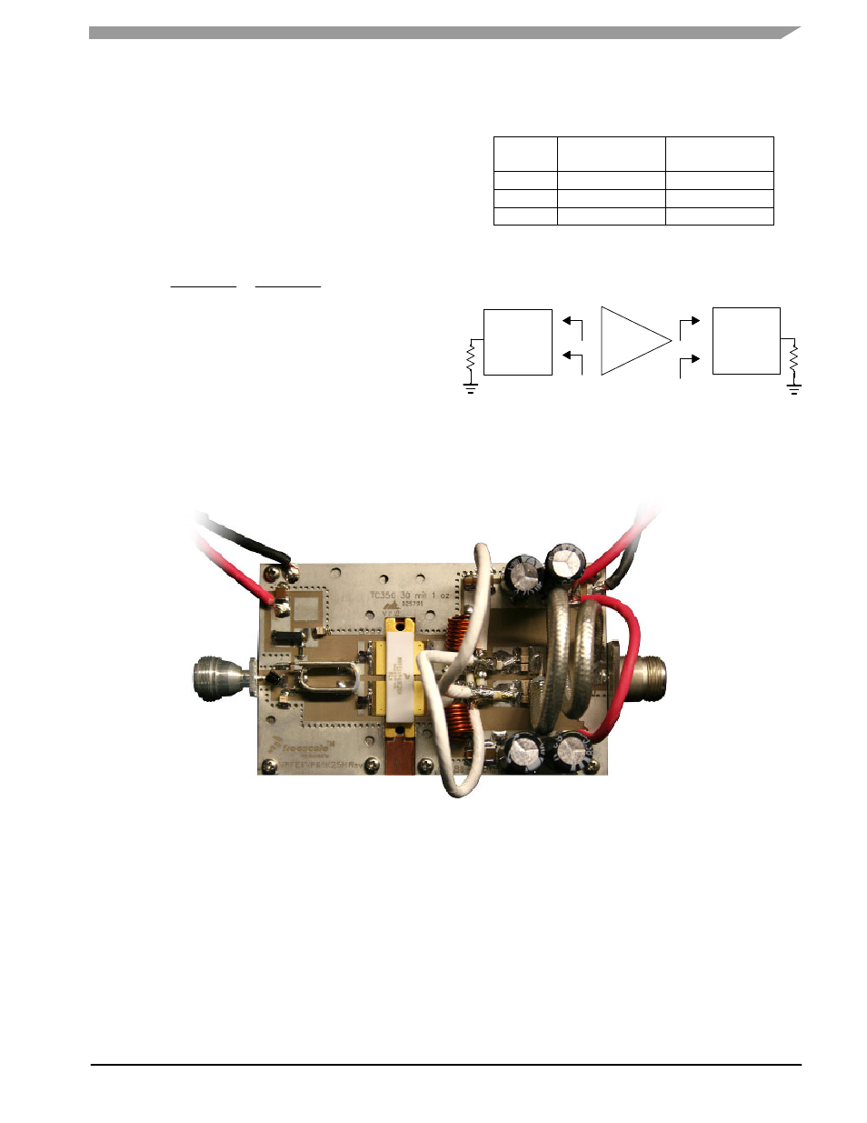
Output
Matching
Network
Input
Matching
Network
Figure 4. Series Equivalent Source and Load
Impedance
Z source
Z load
Device
Under
Test
--
--
+
+
Figure 5. FM Broadcast Reference Design Fixture Impedance