Ap7173, Pin descriptions, Functional block diagram – Diodes AP7173 User Manual
Page 3
AP7173
1.5A LOW DROPOUT LINEAR REGULATOR WITH
PROGRAMMABLE SOFT-START
AP7173
Document number: DS31369 Rev. 9 - 2
3 of 15
April 2011
© Diodes Incorporated
Pin Descriptions
Pin Name
PIN #
Description
SO-8EP
DFN3030-10
IN
1
1, 2
Power Input pin.
PG 2 3
Power-Good pin, open-drain output. When the V
OUT
is below the
PG threshold the PG pin is driven low; when the V
OUT
exceeds the
threshold, the PG pin goes into a high-impedance state. To use the PG
pin, use a 10k
Ω to 1MΩ pull-up resistor to pull it up to a supply of up to
5.5V, which can be higher than the input voltage.
VCC 3 4
Bias Input pin, provides input voltage for internal control circuitry. This
voltage should be higher than the V
IN
.
EN 4 5
Enable pin. This pin should be driven either high or low and must not
be floating. Driving this pin high enables the regulator, while pulling it
low puts the regulator into shutdown mode.
GND 5 6
Ground.
SS 6 7
Soft-Start pin. Connect a capacitor between this pin and the ground to
set the soft-start ramp time of the output voltage. If no capacitor is
connected, the soft-start time is typically 100µS.
FB 7 8
Feedback pin. Connect this pin to an external voltage divider to set the
output voltage.
OUT
8
9, 10
Regulated Output pin.
Thermal Pad
—
—
Solder this pad to large ground plane for increased thermal
performance.
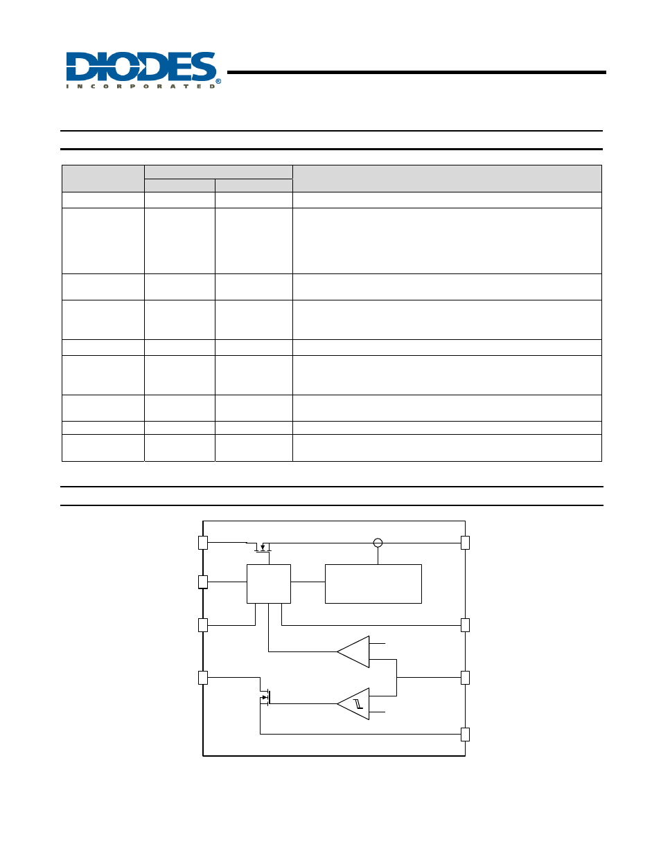
Functional Block Diagram
Gate
Driver
Current Limit and
Thermal Shutdown
0.8V
0.72V
OUT
SS
FB
GND
IN
VCC
PG
EN
+
-
+
-