Diodes AP7173 User Manual
Ap7173, Description, Pin assignments
AP7173
1.5A LOW DROPOUT LINEAR REGULATOR WITH
PROGRAMMABLE SOFT-START
AP7173
Document number: DS31369 Rev. 9 - 2
1 of 15
April 2011
© Diodes Incorporated
Description
The AP7173 is a 1.5A low-dropout (LDO) linear regulator that
features a user-programmable soft-start, an enable input and
a power-good output.
The soft-start reduces inrush current of the load capacitors
and minimizes stress on the input power source during start-
up. The enable input and power-good output allow users to
configure power management solutions that can meet the
sequencing requirements of FPGAs, DSPs, and other
applications with different start-up and power-down
requirements.
The AP7173 is stable with any type of output capacitor of
2.2µF or more. A precision reference and feedback control
deliver 2%
accuracy over load, line, and operating
temperature ranges. The AP7173 is available in both
DFN3030-10 and SO-8EP packages.
Pin Assignments
Features
●
Low V
IN
and wide V
IN
range: 1.0V to 5.5V
●
Bias voltage (V
VCC
) range: 2.7V to 5.5V
●
Low V
OUT
range: 0.8V to 3.3V
●
Low dropout: 165mV typical at 1.5A, V
VCC
= 5V
●
2% accuracy over line, load and temperature range
●
Power-Good (PG) output for supply monitoring and for
sequencing of other supplies
●
Programmable soft-start provides linear voltage startup
●
Bias supply permits low V
IN
operation with good transient
response
●
Stable with any output capacitor
≥ 2.2µF
●
DFN3030-10 and SO-8EP: available in “Green” molding
compound (No Br, Sb)
●
Lead-free finish/ RoHS Compliant (Note 1)
Applications
•
PCs, Servers, Modems, and Set-Top-Boxes
• FPGA
Applications
•
DSP Core and I/O Voltages
• Post-Regulation
Applications
•
Applications With Sequencing Requirements
Note:
1. EU Directive 2002/95/EC (RoHS). All applicable RoHS exemptions applied. Please visit our website at
Typical Application Circuit
EN
PG
VCC
IN
OUT
FB
SS
GND
AP7173
R1
R2
R3
C1
C2
C3
V
OUT
V
IN
V
VCC
C
SS
Figure 1. Typical Application Circuit (Adjustable Output)
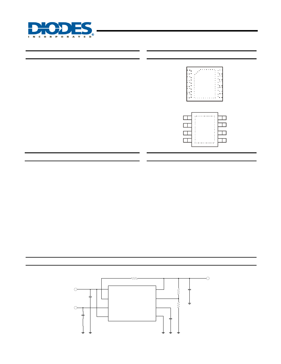
( Top View )
FB
EN
IN
GND
OUT
PG
VCC
IN
SS
OUT
DFN3030-10
1
2
3
4
5
9
10
8
7
6
SO-8EP
SS
VCC
EN
IN
FB
GND
OUT
(Top View)
PG
1
2
3
4
5
6
7
8