Ap7173 – Diodes AP7173 User Manual
Page 10
AP7173
1.5A LOW DROPOUT LINEAR REGULATOR WITH
PROGRAMMABLE SOFT-START
AP7173
Document number: DS31369 Rev. 9 - 2
10 of 15
April 2011
© Diodes Incorporated
Application Notes
BIAS VOLTAGE V
VCC
The AP7173 is a low V
IN
, low dropout regulator that uses
an NMOS pass FET. The VCC pin must be connected to a
DC bias supply V
VCC
for the internal control circuitry and
the gate drive of the pass FET to function properly and to
obtain low dropout. The V
VCC
needs to be equal to or
higher than the V
IN
and in the range of 2.7V-5.5V. Figure
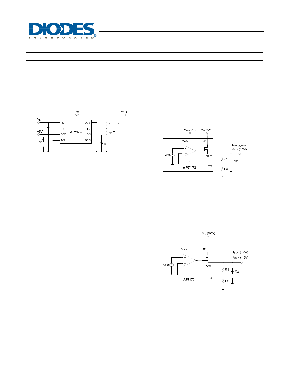
27 illustrates the typical application circuit for the AP7173.
Figure 27. Typical Application Circuit for AP7173
ADJUSTABLE OUTPUT VOLTAGE
With an external voltage divider, the AP7173 can provide
output voltage from 0.8V to 3.3V. R1 and R2 can be
calculated for any output voltage using the following
equation, where V
REF
=0.8 is the AP7173’s internal
reference voltage. Refer to Table 1 for resistor
combinations for commonly used output voltages. For
maximum voltage accuracy, R2 should be
≤ 5kΩ.
V
OUT
= V
REF
x (1 + R1/R2)
INPUT V
IN
AND BIAS V
VCC
CAPACITORS
It is important to keep the IN and VCC pins clear of large
ripples, glitches and other noises by connecting capacitors
to the IN and VCC pins. The required capacitance on these
pins is strongly dependent on source and wiring
impedance of the supplies.
To provide good decoupling for the input power supply V
IN
,
it is recommended that a ceramic capacitor with
capacitance of at least 1
μF is connected between the IN
and GND pins at a location as close to them as possible.
High quality, low ESR capacitors should be used for better
performance.
It is critical to provide good decoupling to the VCC pin for
the AP7173’s internal control circuitry to function properly.
The minimum recommended capacitance for the V
VCC
is
1
μF when the V
VCC
and V
IN
are separate supplies. If the V
IN
and V
VCC
are connected to the same supply, the
recommended minimum capacitance for V
VCC
is 4.7
μF.
Again good quality, low ESR capacitors should be used for
optimum performance.
OUTPUT CAPACITOR
The output capacitor affects the stability and transient
response of the LDO. The AP7173 is designed to be stable
for all types of output capacitors
≥ 2.2μF, single or multiple
in parallel.
Using high quality, low ESR capacitors and placing them
close to the OUT and GND pins can improve perfomance.
DROPOUT VOLTAGE
The very low dropout makes the AP7173 well suited for
high-current, low V
IN
/low V
OUT
applications. To achieve the
specified low-dropout performance for such applications,
the VCC pin should be connected to a separate supply of
at least 3.25V higher than V
OUT
. Figure 28 shows an
application circuit where V
VCC
is 5V and V
OUT
is 1.2V.
Figure. 28 Typical Application Circuit for AP7173
Using Separate VCC and IN Rails
For applications where low dropout is not required or a
separate V
VCC
supply is not available, the IN and VCC pins
can be tied together. In this situation, a voltage difference
of at least 1.7V between the V
VCC
and V
OUT
has to be
maintained for the V
VCC
to provide enough gate drive to
the pass FET. Therefore, the V
OUT
needs to be 1.7V or
more below V
IN
, as shown in Figure 29.
Figure. 29 Typical Application Circuit for AP7173
Without an Auxiliary VCC Rail
PROGRAMMABLE SOFT-START
The AP7173 features a voltage-controlled soft-start that is
programmable with an external capacitor (C
SS
). The
AP7173 achieves a monotonic soft-start by tracking the
voltage ramp of the external soft-start capacitor until the
ramp voltage reaches the internal reference voltage.