Application information, Fv v t, T2l v v i – Diodes AP65550 User Manual
Page 9
AP65550
Document number: DS36336 Rev. 2 - 2
9 of 14
www.diodes.com
April 2014
© Diodes Incorporated
AP65550
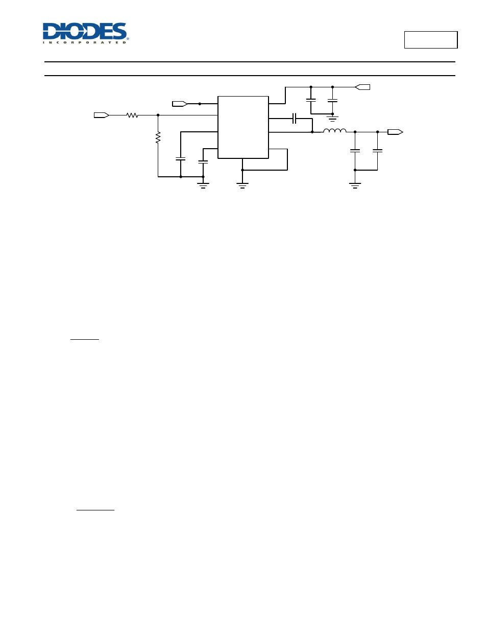
Application Information
EN
FB
VREG5
SS
EP
GND
SW
VIN
BS
8.25K
Ω
22.1K
Ω
1.5µH
EN
VOUT
VIN
VOUT
AP65550
1
2
3
4
5
6
7
8
8.2nF
1µF
10µF
22µF
0.1µF
R3
R1
C4
C6
L1
C1
10µF
C2
C8
22µF
C5
C9
Figure 3. Typical Application of AP65550
PWM Operation and Adaptive On-time Control
The AP65550 is synchronous step-down converters with internal power MOSFETs. Adaptive constant on time (COT) control is employed to
provide fast transient response and easy loop stabilization. At the beginning of each cycle, the high-side MOSFET is turned on. This MOSFET is
turned off after internal one shot timer expires. This one shot is set by the converter input voltage(V
IN
), and the output voltage(V
OUT
) to maintain a
pseudo-fixed frequency over the input voltage range, hence it is called adaptive on-time control. The output voltage variation is sensed by FB
voltage. The one-shot timer is reset and the high-side MOSFET is turned on again when FB voltage falls below the 0.76V.
AP65550 uses an adaptive on-time control scheme and does not have a dedicated in board oscillator. It runs with a pseudo-constant frequency of
650kHz by using the input voltage and output voltage to set the on-time one-shot timer. The on-time is inversely proportional to the input voltage
and proportional to the output voltage. It can be calculated using the following equation:
f
V
V
T
IN
OUT
ON
V
OUT
is the output voltage
V
IN
is the input voltage
f is the switching frequency
After an ON-time period, the AP65550 goes into the OFF-time period. The OFF-time period length depends on VFB in most case. It will end when
the FB voltage decreases and below 0.76V then the ON-time periods is triggered. If the OFF-time period is less than the minimum OFF time, the
minimum OFF time will be applied, which is about 260ns typical.
Power Save Mode
The AP65550 is designed with Power Save Mode (PSM) at light load conditions for high efficiency. The AP65550 automatically reduces the
switching frequency and change the Ton time to Tmin-on time during a light load condition to get high efficiency and low output ripple
.
As the
output current decreases form heavy load condition, the inductor current decreases as well, eventually comes close to zero current, which is the
boundary between CCM and DCM. The low side MOSFET is turned off when the inductor current reaches zero level. The load is provided only by
output capacitor, when FB voltage is lower than 0.76V, the next cycle ON cycle is beginning. The on-time is the minimum on time that benefit for
decreasing V
OUT
ripple at light load condition. When the output current increases from light to heavy load, the switching frequency increases to
keep output voltage. The transition point to light load operation can be calculated using the following equation:
ON
OUT
IN
LOAD
T
2L
V
V
I
T
ON
is on-time
Enable
Above the ‘EN high-level input voltage’, the internal regulator is turned on and the quiescent current can be measured above this threshold. The
enable (EN) input allows the user to control turning on or off the regulator. To enable the AP65550, EN must be pulled above
the ‘EN high-level
input voltage’ and to disable the AP65550, EN must be pulled below ‘EN low-level input voltage’.