Pin descriptions, Functional block diagram – Diodes AP65550 User Manual
Page 2
AP65550
Document number: DS36336 Rev. 2 - 2
2 of 14
www.diodes.com
April 2014
© Diodes Incorporated
AP65550
Pin Descriptions
Pin
Name
Pin Number
Function
SO-8EP
EN
1
Enable input. EN is a digital input that turns the regulator on or off. Drive EN high to turn on the
regulator, drive it low to turn off. Pull
up with 100kΩ resistor for automatic startup.
FB
2
Feedback Input. FB senses the output voltage and regulates it. Drive FB with a resistive voltage
divider connected to it from the output voltage.
VREG5
3
Internal power supply output pin to connect an additional capacitor. Connect a
1μF (typical) capacitor
as close as possible to the VREG5 and GND. This pin is not active when EN is low.
SS
4
Soft-start control input pin. SS controls the soft start period. Connect a capacitor from SS to GND to
set the soft-start period.
GND
5
Ground pin is the main power ground for the switching circuit.
SW
6
Power Switching Output. SW is the switching node that supplies power to the output. Connect the
output LC filter from SW to the output load. Note that a capacitor is required from SW to BS to power
the high-side switch.
BS
7
Bootstrap pin. A bootstrap capacitor is connected between the BS pin and SW pin. The voltage across
the bootstrap capacitor drives the internal high-
side NMOS switch. A 0.1μF (typical) capacitor is
required for proper operation
VIN
8
Supply input pin. A capacitor should be connected between the VIN pin and GND pin to keep the DC
input voltage constant.
EP
—
Connect the exposed thermal pad to GND on the PCB
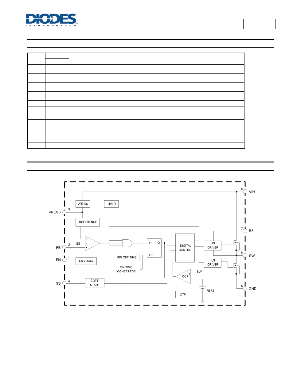
Functional Block Diagram
Figure 2. Functional Block Diagram