Application information, Iv c t – Diodes AP65550 User Manual
Page 10
AP65550
Document number: DS36336 Rev. 2 - 2
10 of 14
www.diodes.com
April 2014
© Diodes Incorporated
AP65550
Application Information
(cont.)
Soft-start
The soft-start time of the AP65550 is programmable by selecting different C
SS
value. When the EN pin becomes high, the C
SS
is charged by a 6μA
current source, generating a ramp signal fed into non-inverting input of the error comparator. Reference voltage V
REF
or the internal soft-start
voltage SS whichever is smaller dominates the behavior of the non-inverting inputs of the error amplifier. Accordingly, the output voltage will follow
the SS signal and ramp up smoothly to its target level. The capacitor value required for a given soft-start ramp time can be expressed as:
SS
FB
SS
SS
I
V
C
t
Where C
SS
is the required capacitor between SS pin and GND, t
SS
is the desired soft-start time and V
FB
is the feedback voltage.
Over Current Protection (OCP)
Figure 4 shows the over current protection (OCP) scheme of AP65550. In each switching cycle, the inductor current is sensed by monitoring the
low-side MOSFET in the OFF period. When the voltage between GND pin and SW pin is smaller than the over current trip level, the OCP will be
triggered and the controller keeps the OFF state. A new switching cycle will begging when the measured voltage is larger than limit voltage. The
internal counter is incremented when OCP is triggered. After 16 sequential cycles, the internal OCL (Over Current Logic) threshold is set to a
lower level, reducing the available output current. When a switching cycle occurs where the switch current is below the lower OCL threshold, the
counter is reset and OCL limit is returned to higher value.
Because the R
DS(ON)
of MOSFET increases with temperature, V
Limit
has xppm/
o
C temperature coefficient to compensate this temperature
dependency of R
DS(ON)
.
OC
COMPARATOR
-266mV
Q1
Q2
S
Q
R
Figure 4. Over Current Protection Scheme
Under Voltage Lockout
The AP65550 provides an under voltage lockout circuit to prevent it from undefined status when startup. The UVLO circuit shuts down the device
when V
IN
drops below 3.45V. The UVLO circuit has 320mV hysteresis, which means the device starts up again when V
REG
rise to 3.75V. (non-
latch)
Thermal shutdown
If the junction temperature of the device reaches the thermal shutdown limit of 160°C, the AP65550 shuts itself off, and both HMOS and LMOS will
be turned off. The output is discharge with the internal transistor. When the junction cools to the required level (130°C nominal), the device initiates
soft-start as during a normal power -up cycle.
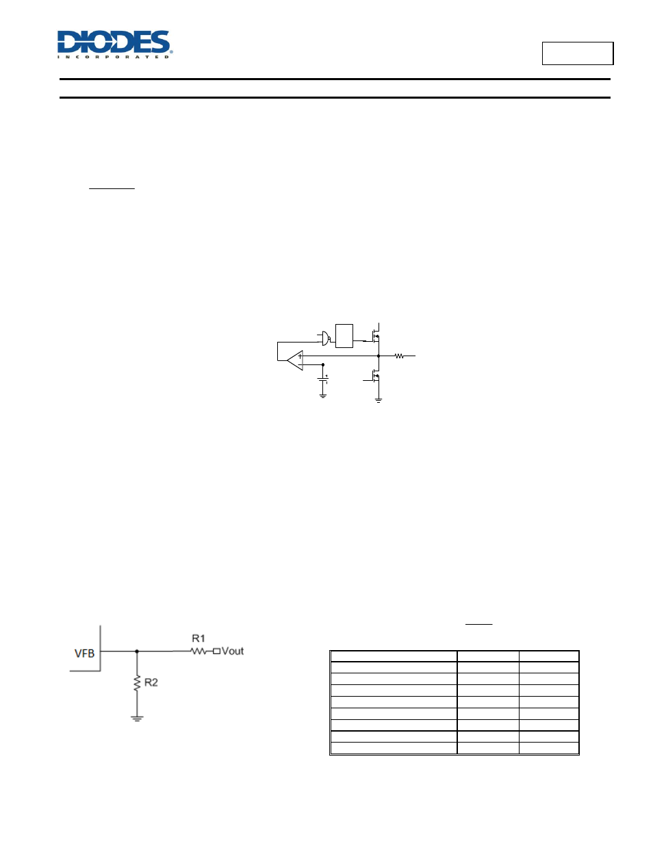
Setting the Output Voltage
The output voltage can be adjusted from 1.000 to 5V using an external resistor divider. Table 1 shows a list of resistor selection for common
output voltages. Resistor R1 is selected based on a design tradeoff between efficiency and output voltage accuracy. For high values of R1 there
is less current consumption in the feedback network. However the trade off is output voltage accuracy due to the bias current in the error
amplifier. R1 can be determined by the following equation:
1
0.765
V
R
R
OUT
2
1
Figure 5. Feedback Divider Network
Output Voltage (V)
R1 (kΩ)
R2 (kΩ)
1
6.81
22.1
1.05
8.25
22.1
1.2
12.7
22.1
1.5
21.5
22.1
1.8
30.1
22.1
2.5
49.9
22.1
3.3
73.2
22.1
5
124
22.1
Table 1. Resistor Selection for Common Output
Voltages