Zxld1371, Electrical characteristics – Diodes ZXLD1371 User Manual
Page 6
ZXLD1371
ZXLD1371
Document number: DS35436 Rev. 1 - 2
6 of 42
February 2012
© Diodes Incorporated
A Product Line of
Diodes Incorporated
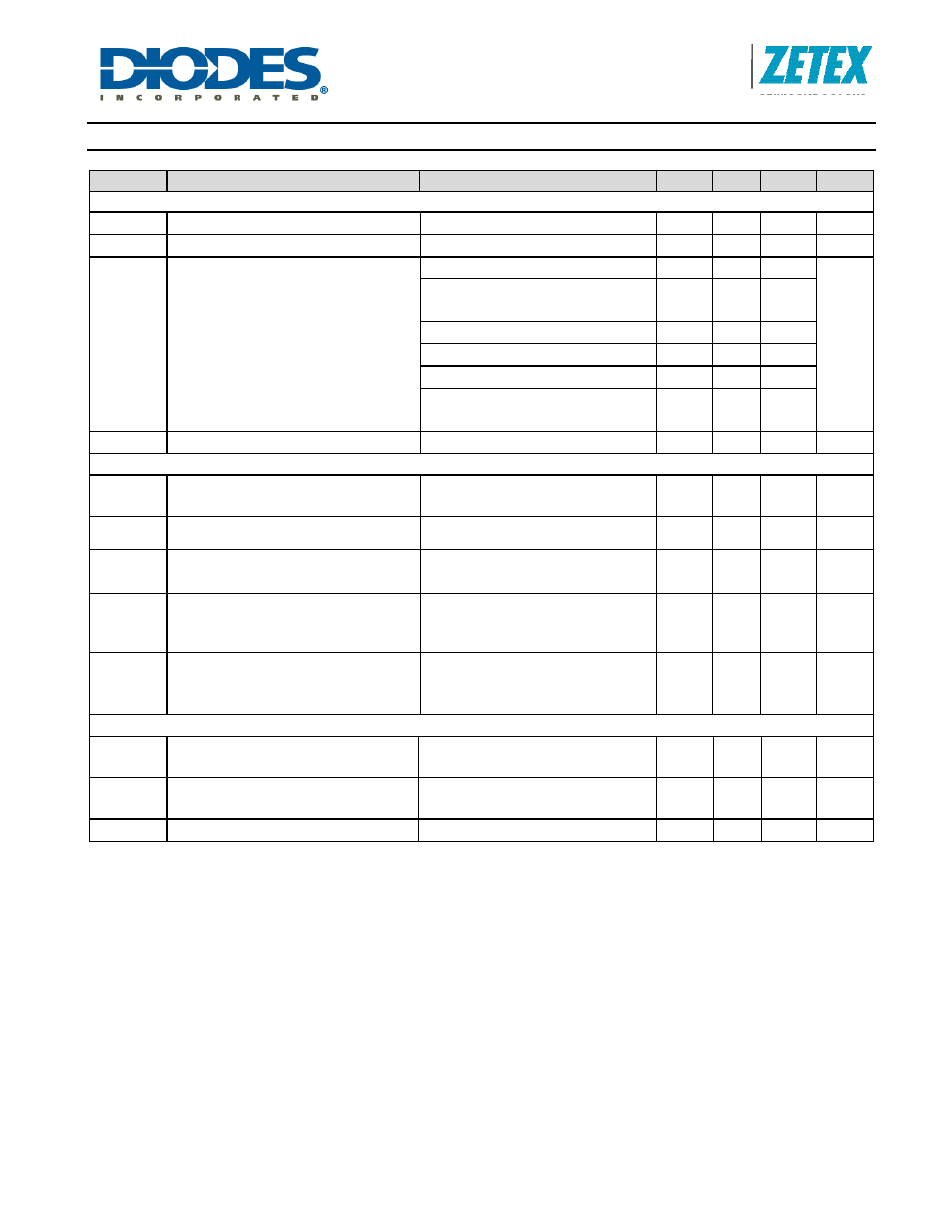
Electrical Characteristics
(cont.)
(Test conditions: V
IN
= V
AUX
= 12V, T
A
= 25°C, unless otherwise specified.)
Symbol
Parameter
Conditions
Min
Typ
Max
Units
Output Parameters
V
FLAGL
FLAG pin low level output voltage
Output sinking 1mA
0.5
V
I
FLAGOFF
FLAG pin open-drain leakage current
V
FLAG
= 40V
1
µA
V
STATUS
STATUS Flag no-load output voltage
(Note 10)
Normal operation
4.2
4.5
4.8
V
Out of regulation (V
SHP
out of range)
(Note 11)
3.3
3.6
3.9
V
IN
under-voltage (V
IN
< UVLO)
3.3
3.6
3.9
Switch stalled (t
ON
or t
OFF
> 100µs)
3.3
3.6
3.9
Over-temperature (T
J
> 125°C)
1.5
1.8
2.1
Excess sense resistor current
(V
SENSE
> 0.32V)
0.6
0.9
1.2
R
STATUS
Output impedance of STATUS output
Normal operation
10
k
Ω
Driver output (PIN GATE)
V
GATEH
High level output voltage
No load Sourcing 1mA
(Note 12)
10 11
V
V
GATEL
Low level output voltage
Sinking 1mA, (Note 13)
0.5
V
V
GATECL
High level GATE CLAMP voltage
V
IN
= V
AU X
= V
ISM
= 18V
I
GATE
= 1mA
12.8
15 V
I
GATE
Dynamic peak current available during
rise or fall of output voltage
Charging or discharging gate of
external switch with Q
G
= 10nC and
400kHz
±300 mA
t
STALL
Time to assert ‘STALL’ flag and
warning on STATUS output
(Note 14)
GATE low or high
100
170
µs
LED Thermal control circuit (T
ADJ
) parameters
V
TADJH
Upper threshold voltage
Onset of output current reduction
(V
TADJ
falling)
560
625
690
mV
V
TADJL
Lower threshold voltage
Output current reduced to <10% of
set value (V
TADJ
falling)
380
440
500
mV
I
TADJ
T
ADJ
pin Input current
V
TADJ
= 1.25V
1
µA
Notes:
10. In the event of more than one fault/warning condition occurring, the higher priority condition will take precedence.
For example ‘Excessive coil current’ and ‘Out of regulation’ occurring together will produce an output of 0.9V on the STATUS pin.
These STATUS pin voltages apply for an input voltage to V
IN
of 7.5V < V
IN
< 60V. Below 7.5V the STATUS pin voltage levels reduce and
therefore may not report the correct status. For 5.4V < V
IN
< 7.5V the flag pin still reports any error by going low. At low V
IN
in Boost and
Buck-boost modes an over-current status may be indicated when operating at high boost ratios – this due to the feedback loop increasing
the sense voltage.
For more information see the Application Information section about Flag/Status levels.
11. Flag is asserted if V
SHP
< 1.5V or V
SHP
> 2.5V
12. GATE is switched to the supply voltage V
AUX
for low values of V
AUX
(5V
≤ V
AUX
≤ ~12V). For V
AUX
> 12V, GATE is clamped internally to prevent
it exceeding 15V.
13. GATE is switched to PGND by an NMOS transistor
14. If t
ON
exceeds t
STALL
, the device will force GATE low to turn off the external switch and then initiate a restart cycle. During this phase, ADJ is
grounded internally and the SHP pin is switched to its nominal operating voltage, before operation is allowed to resume. Restart cycles will be
repeated automatically until the operating conditions are such that normal operation can be sustained. If t
OFF
exceeds t
STALL
, the switch will
remain off until normal operation is possible.