Zxld1371, Package thermal data, Recommended operating conditions – Diodes ZXLD1371 User Manual
Page 4
ZXLD1371
ZXLD1371
Document number: DS35436 Rev. 1 - 2
4 of 42
February 2012
© Diodes Incorporated
A Product Line of
Diodes Incorporated
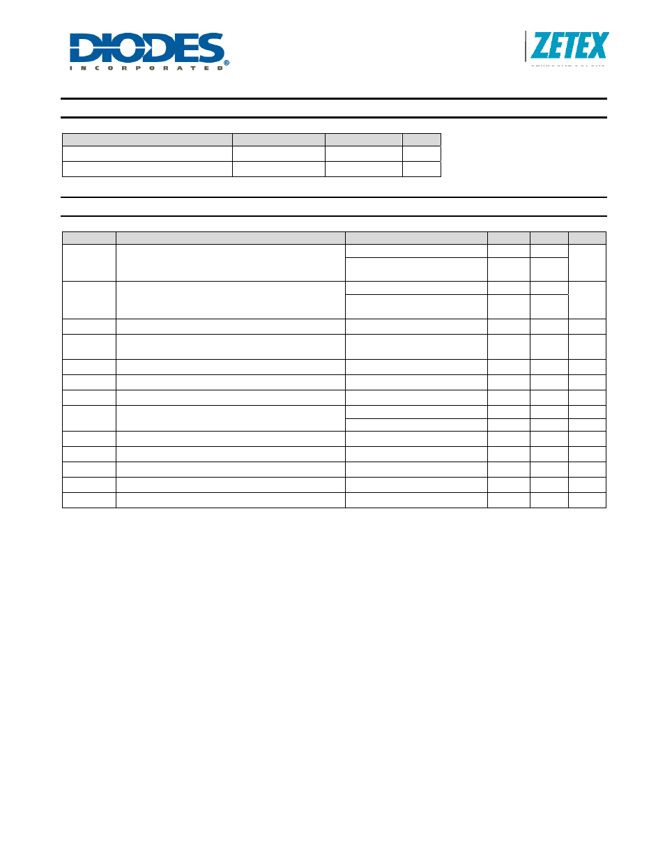
Package Thermal Data
Thermal Resistance
Package
Typical
Unit
Junction-to-Ambient,
θ
JA
(Note 4)
TSSOP-16 EP
50
°C/W
Junction-to-Case,
θ
JC
TSSOP-16 EP
23
°C/W
Recommended Operating Conditions
(-40°C
≤ T
J
≤ 125°C)
Symbol
Parameter
Performance/Comment
Min
Max
Unit
V
IN
Input supply voltage range
Normal Operation
8.0
60
V
(Note 5) Reduced performance
operation
5.0 8.0
V
AUX
Auxiliary supply voltage range (Note 6)
Normal Operation
8.0
60
V
(Note 5) Reduced performance
operation
5.0
8.0
V
SENSE
Differential input voltage
V
IN
-V
ISM
, with 0
≤ V
ADJ
≤ 2.5
0
450
mV
V
ADJ
External dc control voltage applied to ADJ pin to
adjust output current
DC brightness control mode
from 10% to 100%
0.125 1.25
V
I
REF
Reference external load current
REF sourcing current
1
mA
f
max
Recommended switching frequency range
(Note 7) 300
1000
kHz
V
TADJ
Temperature adjustment (T
ADJ
) input voltage range 0
V
REF
V
f
PWM
Recommended PWM dimming frequency range
To achieve 1000:1 resolution
100
500
Hz
To achieve 500:1 resolution
100
1000
Hz
t
PWMH/L
PWM pulse width in dimming mode
PWM input high or low
0.002
10
ms
V
PWMH
PWM pin high level input voltage
2
5.5
V
V
PWML
PWM pin low level input voltage
0
0.4
V
T
J
Operating Junction Temperature Range
-40
125
°C
GI
Gain setting ratio for boost and buck-boost modes Ratio= V
GI
/V
ADJ
0.20 0.50
Notes: 3.
For
correct operation SGND and PGND should always be connected together.
4. Measured on “High Effective Thermal Conductivity Test Board" according to JESD51.
5. Device starts up above 5.4V and as such the minimum applied supply voltage has to be above 5.4V (plus any noise margin). The ZXLD1371 will,
however, continue to function when the input voltage is reduced from
≥ 8V down to 5.0V.
When operating with input voltages below 8V the output current and device parameters may deviate from their normal values; and is dependent
on power MOSFET switch, load and ambient temperature conditions. To ensure best operation in Boost and Buck-boost modes with input
voltages, V
IN
, between 5.0 and 8V a suitable boot-strap network on V
AUX
pin is recommended.
Performance in Buck mode will be reduced at input voltages (V
IN
, V
AUX
) below 8V. – a boot-strap network cannot be implemented in buck mode.
6.
V
AUX
can be driven from a voltage higher than V
IN
to provide higher efficiency at low V
IN
voltages, but to avoid false operation; a voltage should
not be applied to V
AUX
in the absence of a voltage at V
IN
. V
AUX
can also be operated at a lower voltage than V
IN
to increase efficiencies at high
V
IN
.
7. The device contains circuitry to control the switching frequency to approximately 400kHz. The maximum and minimum operating frequency is not
tested in production.