Zxld1371, Pin descriptions – Diodes ZXLD1371 User Manual
Page 2
ZXLD1371
ZXLD1371
Document number: DS35436 Rev. 1 - 2
2 of 42
February 2012
© Diodes Incorporated
A Product Line of
Diodes Incorporated
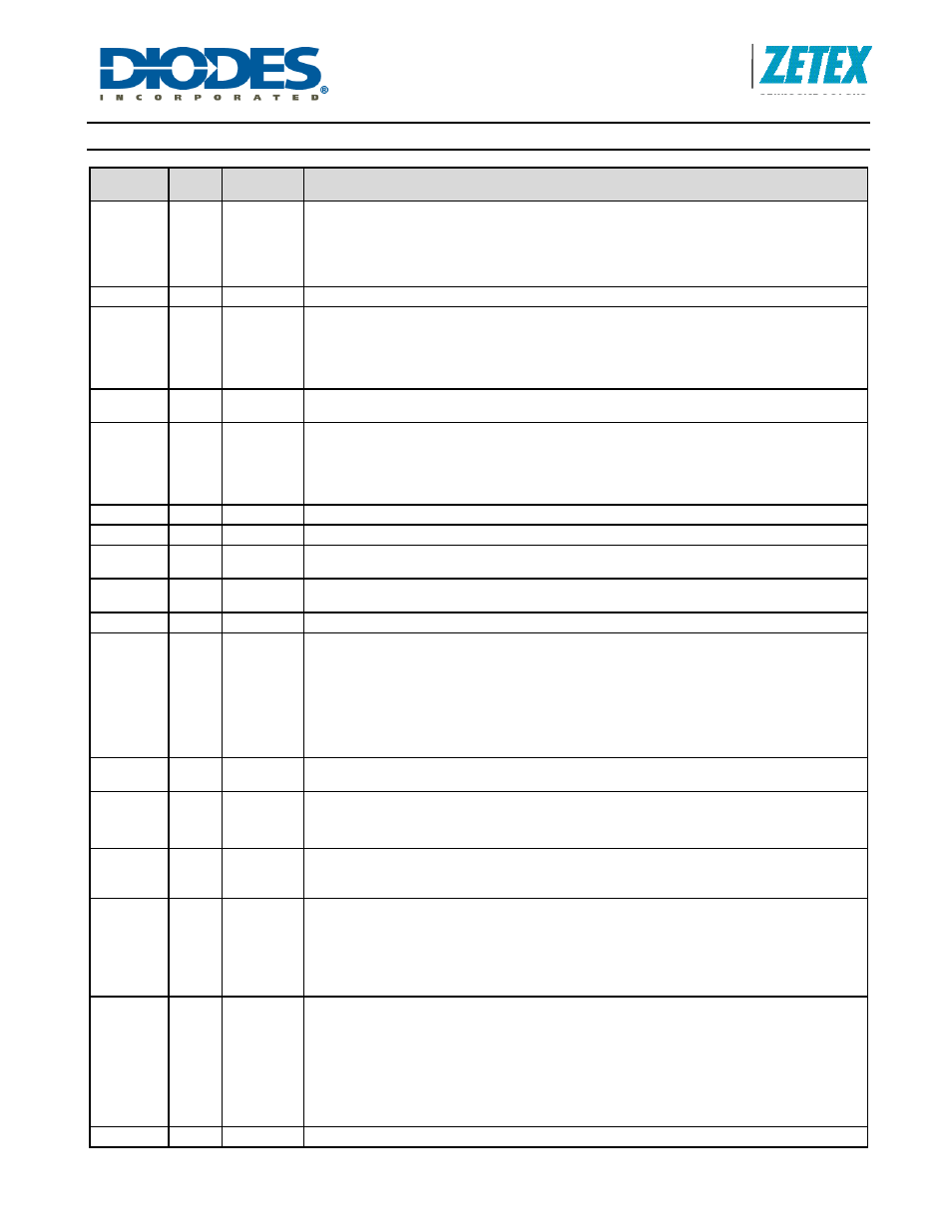
Pin Descriptions
Pin
Name
Pin
Type
(Note 2)
Description
ADJ 1 I
Adjust input (for dc output current control) ADJ < 1.25V) to adjust output current from 10% to 100% of set value. The ADJ pin has an internal clamp that limits the internal node to less than 3V. This provides some failsafe should they get overdriven REF 2 O Internal 1.25V reference voltage output TADJ 3 I Temperature Adjust input for LED thermal current control Connect to REF to disable thermal compensation function. (See section on thermal control.) SHP 4 I/O Shaping capacitor for feedback control loop STATUS 5 O Operation status output (analog output) SGND 6 P Signal ground (Connect to 0V) PGND 7 P Power ground - Connect to 0V and pin 8 to maximize copper area N/C 8 - Not Connected internally – recommend connection to pin 7, (PGND), to maximize PCB copper for thermal dissipation N/C 9 Not Connected internally – recommend connection pin 10 (GATE) to permit wide copper trace to gate of MOSFET GATE 10 O Gate drive output to external NMOS transistor – connect to pin 9 V AUX 11 P Auxiliary positive supply to internal switch gate driver IN < 8V; a bootstrap circuit is recommended to ensure adequate gate drive voltage (see Applications section) IN > 8V; connect to V IN At V IN >24V; to reduce power dissipation, V AUX can be connected to an 8V to 15V auxiliary power supply (see Applications section). Decouple to ground with capacitor V IN 12 P Input supply to device 5V to 60V ISM 13 I Current monitor input. Connect current sense resistor between this pin and V IN The nominal voltage, V SENSE , across the resistor is 218mV fixed in Buck mode and initially 225mV in Boost and Buck-Boost modes, varying with duty cycle. FLAG 14 O Flag open drain output PWM 15 I Digital PWM output current control GI 16 I Gain setting input node to less than 3V. This provides some failsafe should it become overdriven. EP PAD P Exposed paddle. Connect to 0V plane for electrical and thermal management Notes: 2. Type refers to whether or not pin is an Input, Output, Input/Output or Power supply pin.
Connect to REF to set 100% output current.
Drive with dc voltage (125mV
Connect thermistor/resistor network to this pin to reduce output current above a preset
temperature threshold.
Connect 330pF ±20% capacitor from this pin to ground to provide loop compensation
Pin is at 4.5V (nominal) during normal operation.
Pin switches to a lower voltage to indicate specific operation warnings or fault
conditions. (See section on STATUS output.)
Status pin voltage is low during shutdown mode
At V
At V
close to device (see Applications section)
Decouple to ground with capacitor close to device (refer to Applications section)
Pin is high impedance during normal operation
Pin switches low to indicate a fault, or warning condition
Pin driven either by open Drain or push-pull 3.3V or 5V logic levels.
Drive with frequency higher than 100Hz to gate output ‘on’ and ‘off’ during dimming
control.
The device enters standby mode when PWM pin is driven with logic low level for more
than 15ms nominal (Refer to application section for more details)
Used to set the device in Buck mode or Boost, Buck-boost modes and to control the
sense voltage in Boost and Buck-boost modes
Connect to ADJ pin for Buck mode operation
For Boost and Buck-boost modes, connect to resistive divider from ADJ to SGND. The
GI divider is required to compensate for duty cycle gating in the internal feedback loop
(see Application section). The GI pin has an internal clamp that limits the internal