Zxld1371, Applications information – Diodes ZXLD1371 User Manual
Page 30
ZXLD1371
ZXLD1371
Document number: DS35436 Rev. 1 - 2
30 of 42
February 2012
© Diodes Incorporated
A Product Line of
Diodes Incorporated
Applications Information
(cont.)
Example 2)
Using the ZXMN6A09K (V
DS(MAX)
= 60V, I
D(MAX)
= 12.2A):
Æ Q
G
= 29nC at V
GS
= 10V
ZXLD1371 I
PEAK
= 300mA
Assuming that cumulatively the rise time and fall time can account for a maximum of 10% of the period, the maximum
frequency allowed in this condition is:
t
PERIOD
= 20*dt
Æ
f = 1/ t
PERIOD
= 515kHz
This frequency is within the recommended frequency range the device can handle, therefore the ZXMN6A09K is
recommended to be used with the ZXLD1371 for frequencies from 300kHz to 500kHz).
The recommended total gate charge for the MOSFET used in conjunction with the ZXLD1371 is less than 30nC.
Junction Temperature Estimation
Finally, the ZXLD1371 junction temperature can be estimated using the following equations:
Total supply current of ZXLD1371:
I
QTOT
≈ I
Q
+ f • Q
G
Where
I
Q
= total quiescent current I
Q-IN
+ I
Q-AUX
Power consumed by ZXLD1371
P
IC
= V
IN
• (I
Q
+ f • Qg)
Or in case of separate voltage supply, with V
AUX
< 15V
P
IC
= V
IN
• I
Q-IN
+ V
aux
• (I
Q-AUX
+ f • Qg)
T
J
=
T
A
+ P
IC
•
θ
JA
=
T
A
+ P
IC
• (
θ
JC
+
θ
CA)
Where the total quiescent current I
QTOT
consists of the static supply current (I
Q
) and the current required to charge and
discharge the gate of the power MOSFET. Moreover the part of thermal resistance between case and ambient depends on
the PCB characteristics.
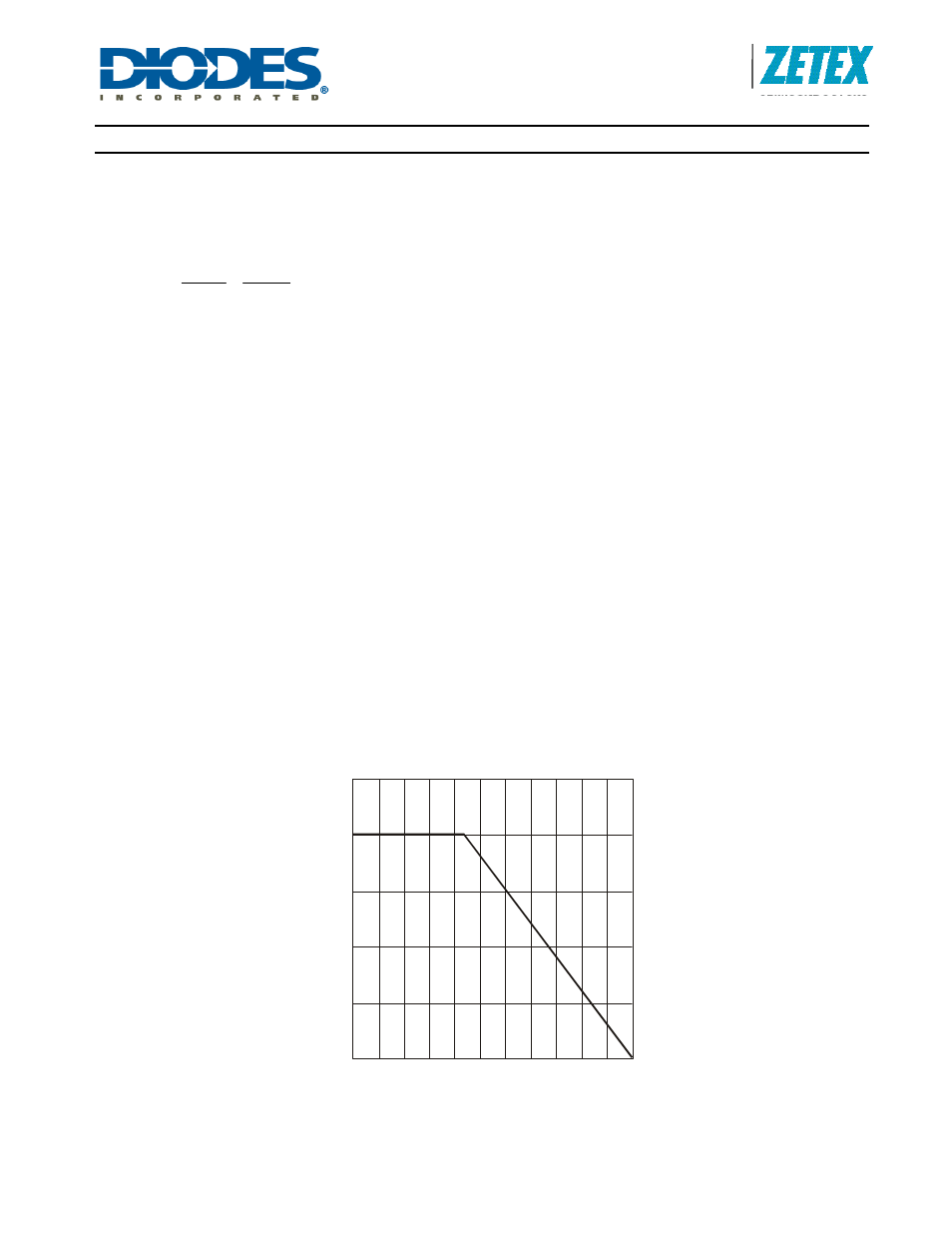
Figure 8. Power derating curve for ZXLD1370
mounted on test board according to JESD51
ns
97
mA
300
nC
29
PEAK
I
g
Q
dt
=
=
=
0
0.5
1
1.5
2
2.5
-40 -25 -10
5
20
35 50
65 80 95 110 125
AMBIENT TEMPERATURE (°C)
P
O
WE
R
D
IS
S
IP
A
T
IO
N (
m
W
)