Zxld1371, Applications information (cont.), Shp pin v – Diodes ZXLD1371 User Manual
Page 40: Decoupling inductor, switch and freewheeling diode
ZXLD1371
ZXLD1371
Document number: DS35436 Rev. 1 - 2
40 of 42
February 2012
© Diodes Incorporated
A Product Line of
Diodes Incorporated
Applications Information (cont.)
PCB Layout Considerations
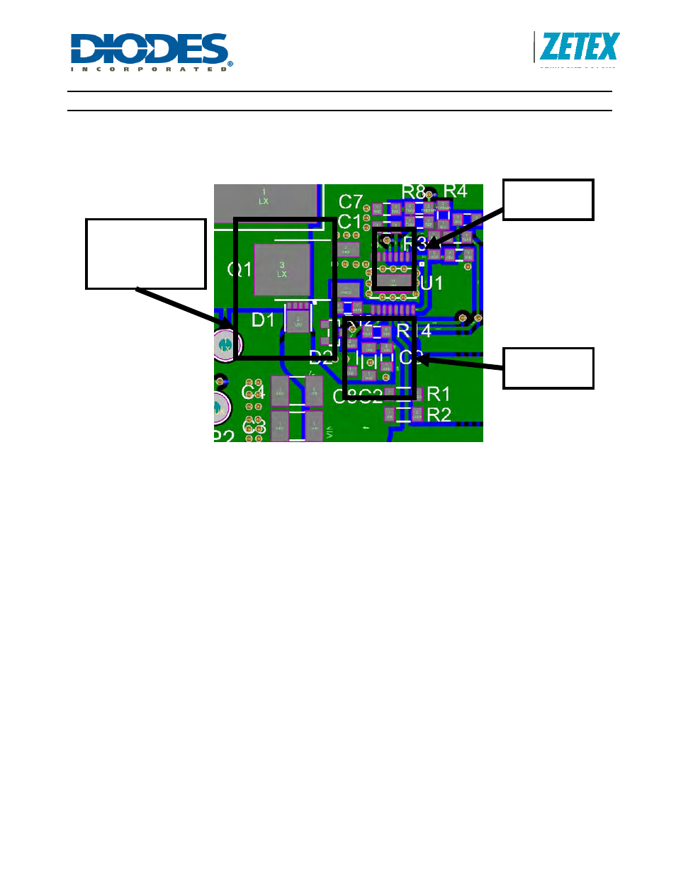
PCB layout is a fundamental to device performance in all configurations. Figure 20 shows a section of a proven
ZXLD1371 PCB layout.
Figure 20. Circuit Layout
Here are some considerations useful for the PCB layout using ZXLD1371 in Buck, Boost and Buck-boost configurations:
In order to avoid ringing due to stray inductances, the inductor L1, the anode of D1 and the drain of Q1 should be
placed as close together as possible.
The shaping capacitor C1 is fundamental for the stability of the control loop. To this end it should be placed no
more than 5mm from the SHP pin.
Input voltage pins, VIN and VAUX, need to be decoupled. It is recommended to use two ceramic capacitors of
2.2uF, X7R, 100V (C3 and C4). In addition to these capacitors, it is suggested to add two ceramic capacitors of
1uF, X7R, 100V each (C2, C8), as well as a further decoupling capacitor of 100nF close to the VIN/VAUX pins
(C9). VIN and VAUX pins can be short-circuited when the device is used in buck mode, or can be driven from a
separate supply.
The underside of the PCB should be a solid copper ground plane, electrically bonded to top ground copper at
regular intervals using plated-thro via holes. The ground plane should be unbroken as far as possible, particularly
in the area of the switching circuit including the ZXLD1371, L1, Q1 D, C3 and C4. Plated via holes are necessary
to provide a short electrical path to minimize stray inductance. Critical positions of via holes include the decoupling
capacitors, the source connection of the MOSFET and the ground connections of the ZXLD1371, including the
centre paddle. These via holes also serve to conduct heat away from the semiconductors and minimize the device
junction temperatures.
Evaluation Boards
To support easier evaluation of the ZXLD1371 three evaluation boards have been developed which available via your
Diodes sales representative for qualified opportunities:
ZXLD1371EV1 Buck
configuration
ZXLD1371EV2 Buck-boost
configuration
ZXLD1371EV3 Boost
configuration
SHP pin
V
IN
/ V
AUX
decoupling
Inductor, Switch
and
Freewheeling
diode