Rainbow Electronics MAX3420E User Manual
Page 19

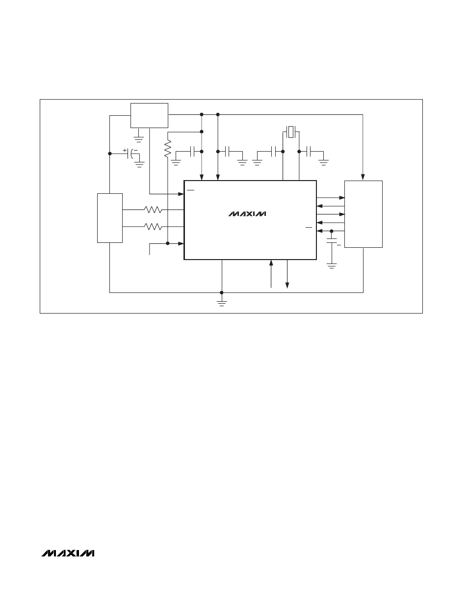
MAX3420E in a Bus-Powered Application
Figure 16 depicts the MAX3420E in a peripheral device
that is powered by V
BUS
. This configuration is advanta-
geous because it requires no external power supply.
V
BUS
is specified from 4.75V–5.25V, so a 3.3V regulator
is required to power the MAX3420E. This diagram
assumes that the microprocessor is powered by 3.3V
as well, so the V
L
pin (logic-level reference voltage) is
connected to V
CC
. Therefore, the GPIO (general-pur-
pose inputs/outputs) are referenced to 3.3V.
USB is a hot-plug system (V
BUS
is hot when the device
is plugged in), so it is good design practice to use a
power-on reset circuit to provide a clean reset to the
system when the device is plugged in. The MAX6349TL
serves as an excellent USB regulator, since it has very
low-quiescent current and a POR circuit built in.
Because this design is bus powered, it is not necessary
to test for the presence of V
BUS
. In this case, the bus
voltage-detection input, VBCOMP, makes an excellent
general-purpose input when pulled up to V
L
. The
VBCOMP input has two interrupts associated with it,
VBUSIRQ and NOVBUSIRQ. These interrupts can detect
both edges of any transitions on the VBCOMP input.
The configuration in Figure 16 shows the SPI interface
using the maximum number of SPI interface pins. The
data pins, MOSI and MISO, are separate, and the
MAX3420E supplies an interrupt signal through the INT
output pin to the µP to notify the µP when its attention
is required.
MAX3420E in a Self-Powered Application
Figure 17 shows a self-powered design in which the µP
has its own power source. This is a common configura-
tion in battery-powered handheld devices. Figure 17
also illustrates the SPI interfacing with the minimum
number of pins. This is achieved by using a single bidi-
rectional data line and no interrupt pin connection. The
MAX3420E register bit, FDUPSPI, configures the SPI
interface for bidirectional operation.
Although the system side is shown as powered by
2.5V, the MAX3420E actually accepts interface volt-
ages of 1.71V to 3.6V. By connecting the system sup-
ply voltage to V
L
, the level translators inside the
MAX3420E adjust the GPIO and SPI bus pins to use the
V
L
reference, in this case 2.5V.
The V
BUS
detect input, VBCOMP, is an important
MAX3420E feature. Because the µP is powered
MAX3420E
USB Peripheral Controller
with SPI Interface
______________________________________________________________________________________
19
MAX3420E
V
CC
V
L
XI
XO
INT
MOSI
MISO
SCLK
RES
D+
D-
D+
D-
VBCOMP
SS
0.1
µF
10k
Ω
GPI
GND
V
BUS
33
Ω
33
Ω
1.0
µF
CERAMIC
C
XI
C
XO
12MHz
3.3V
REGULATOR
MAX6349TL
µP
4
4
USB
"B" CONNECTOR
C
SS
33pF*
GND
GPIN GPOUT
4.7
µF
Figure 16. MAX3420E in a Bus-Powered Application
*33pF CAPACITOR WILL NOT BE REQUIRED AFTER REDESIGN.
